So i built OTL direct coupled electrostatics with some decent woofers and i needed a proper XO. I love Jfets. I got them everywhere. I even got them in my purse. Dunno for what, but i'm prepared for the unknown ;-)
However, bored of DSPs and bored of turning XO knobs the whole day instead of listening, i started to design a Jfet buffered PLLXO. Thing is i like my stuff minimal. Also i have a specal affair with single ended 2SK170s. I know i'm not the first to create a Jfet buffered XO and i know Nelson has the genius 6-24 J113 ready for sale. Not saying that's bad, i love it. But i like to etch stuff myself. Single ended, single layered cool old skool. No China. Strictly.
I didn't use CCS in this design. I am using 2SK170 with bias resistors all the time and with a good PSU i have no issues. Noise from my OTL amps is louder than the Jfets anyways. And honestly i never had audible noise from the Jfets even with my headphones. Also i want to use 2SK170BL. These are rare and expensive.
Please bear with me i'm more enthusiast than a pro. Work is still in progress. Also i'm still on a learnig curve in KiCad. I tried it all on a perf board and it worked.
I'm sharing the KiCad files with you for giving back SOMETHING to the community after a decade of silent reading. Also i hope smarter people than me will pick this up and make it something even better. There is potential for that and as said the PCBs are not perfect yet, tho working. There has been the Adason PLLXO, but i found the design still too complicated for no reason (complimentary Jfet pairs and dual rails and still decoupling caps).
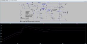
So. This is the 'Vulture' Jfet buffered PLLXO. I called it so because the schematic looks like an abstract vulture ( you need a bit of phantasy for that) 🙂. You can build it in dual mono if you wish. Everything is prepared for that. You will need 6x 2SK170BL matched @10mA. Actually everything between 9 to 11mA should work fine. There is also a PSU using the LM7812. Can be substituted with the 340-12 which is better on paper. There are quite a bunch of caps, probably makes Nelson smile when he sees that. The transfo is an encapsulated Talema 70063K toroid with 2*115V / 2*15V. It's wired for 230V but can easily be changed for the US.
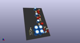
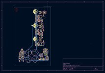
The PCBs are 160x100mm Euro format. There are Hammond enclosures for this form factor. I did not include fuses in the schematic/PCBs because i like to use fuse holders which allow access from the outside of the case. So don't forget your fuses.
The PLLXO itself is first order. You can easily make it second order by adding another PLLXO stage between the buffers / after the first stage. It's really easy. Just use the same parts. 6db+6db makes 12db/Oct.
I think you can't make this any simpler. It's really just a few parts that make a superb active crossover. The right thing for minimalists. Actually you can make this a complete preamp with nearly unity gain by just adding another stage of Jfets and a 50k stereo pot. Maybe add a source selector and you're good as long your source is loud enough.
Did i forget anything? Ah yeah...How to calculate the values for the XO and where to place them. You need to place four devices:
R_HP = Resistor High Pass
C_HP = Cap High Pass
R_LP = Resistor Low Pass
C_LP = Cap Low Pass
Here is a website that shows how PLLXO (passive line level crossover) work and how to calculate the values.
PLLXO
Jfets typically have very high input impedance. It depends a bit on the IDSS of the Jfets you are using. I recommend to start with C=0.1uf and R=10k and see where it takes you. I'm getting around 200Hz with that config.
I used quite big footprints for the PLLXO parts, so that people with love for PIO caps etc have bit of playground.
Pardon me in advance for delayed replies. I'm self employed... Also keep in mind, there can still be issues with the original schematics. I still didnt etch it but only build it on perf board.
Have Fun!
However, bored of DSPs and bored of turning XO knobs the whole day instead of listening, i started to design a Jfet buffered PLLXO. Thing is i like my stuff minimal. Also i have a specal affair with single ended 2SK170s. I know i'm not the first to create a Jfet buffered XO and i know Nelson has the genius 6-24 J113 ready for sale. Not saying that's bad, i love it. But i like to etch stuff myself. Single ended, single layered cool old skool. No China. Strictly.
I didn't use CCS in this design. I am using 2SK170 with bias resistors all the time and with a good PSU i have no issues. Noise from my OTL amps is louder than the Jfets anyways. And honestly i never had audible noise from the Jfets even with my headphones. Also i want to use 2SK170BL. These are rare and expensive.
Please bear with me i'm more enthusiast than a pro. Work is still in progress. Also i'm still on a learnig curve in KiCad. I tried it all on a perf board and it worked.
I'm sharing the KiCad files with you for giving back SOMETHING to the community after a decade of silent reading. Also i hope smarter people than me will pick this up and make it something even better. There is potential for that and as said the PCBs are not perfect yet, tho working. There has been the Adason PLLXO, but i found the design still too complicated for no reason (complimentary Jfet pairs and dual rails and still decoupling caps).
So. This is the 'Vulture' Jfet buffered PLLXO. I called it so because the schematic looks like an abstract vulture ( you need a bit of phantasy for that) 🙂. You can build it in dual mono if you wish. Everything is prepared for that. You will need 6x 2SK170BL matched @10mA. Actually everything between 9 to 11mA should work fine. There is also a PSU using the LM7812. Can be substituted with the 340-12 which is better on paper. There are quite a bunch of caps, probably makes Nelson smile when he sees that. The transfo is an encapsulated Talema 70063K toroid with 2*115V / 2*15V. It's wired for 230V but can easily be changed for the US.
The PCBs are 160x100mm Euro format. There are Hammond enclosures for this form factor. I did not include fuses in the schematic/PCBs because i like to use fuse holders which allow access from the outside of the case. So don't forget your fuses.
The PLLXO itself is first order. You can easily make it second order by adding another PLLXO stage between the buffers / after the first stage. It's really easy. Just use the same parts. 6db+6db makes 12db/Oct.
I think you can't make this any simpler. It's really just a few parts that make a superb active crossover. The right thing for minimalists. Actually you can make this a complete preamp with nearly unity gain by just adding another stage of Jfets and a 50k stereo pot. Maybe add a source selector and you're good as long your source is loud enough.
Did i forget anything? Ah yeah...How to calculate the values for the XO and where to place them. You need to place four devices:
R_HP = Resistor High Pass
C_HP = Cap High Pass
R_LP = Resistor Low Pass
C_LP = Cap Low Pass
Here is a website that shows how PLLXO (passive line level crossover) work and how to calculate the values.
PLLXO
Jfets typically have very high input impedance. It depends a bit on the IDSS of the Jfets you are using. I recommend to start with C=0.1uf and R=10k and see where it takes you. I'm getting around 200Hz with that config.
I used quite big footprints for the PLLXO parts, so that people with love for PIO caps etc have bit of playground.
Pardon me in advance for delayed replies. I'm self employed... Also keep in mind, there can still be issues with the original schematics. I still didnt etch it but only build it on perf board.
Have Fun!
Attachments
Today i found some issues in the first design. So i updated the schematic and PCB files. I also added a ground plane to the crossover. Will update the PSU soon.
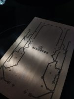
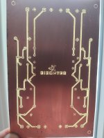
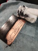
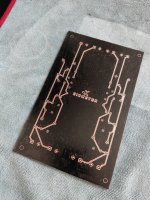
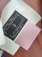
I etched the crossover PCB today. I used the toner transfer method and got a very good result i think. Also i added my name to the PCB. Because it sounds better when my name is on it. That's why manufacturers put their name on their devices. It just sounds better.
However, you can anytime remove it. Not sure if it will even show up on systems without the logo footprint installed.
Maybe it's a good idea to directly solder the components on the copper back. Then it's easier to change PLLXO values.
I still find it a bit difficult to work with KiCad. The tracing is still not perfectly symmetrical. But at least i managed to make the overall layout less confusing with shorter signal paths. I would be grateful if anyone with more experience could clean this up.
Attachments
-
 IMG_20230928_125947.jpg241 KB · Views: 132
 -
 IMG_20230928_125722.jpg271.3 KB · Views: 130
 -
 IMG_20230928_125230.jpg614.9 KB · Views: 125
 -
 IMG_20230928_124154.jpg165.3 KB · Views: 125
 -
 IMG_20230928_123416.jpg196.3 KB · Views: 119
 -
 IMG_20230928_123347.jpg619.7 KB · Views: 127
 -
 IMG_20230928_120925.jpg325.6 KB · Views: 126
 -
 IMG_20230928_120149.jpg124.9 KB · Views: 115
 -
 IMG_20230928_120120.jpg217 KB · Views: 123
 -
 IMG_20230928_113738.jpg249.1 KB · Views: 122
 -
The Vulture Jfet Buffer - XO V1.1.zip3.1 MB · Views: 115
Last edited:
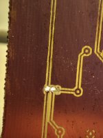
V1.1 went wrong while drilling the PCB. I should have used bigger pads for the Jfets. Oh well...
Actually maybe not that bad. I already mentioned it would be nicer to have the CU on top of the PCB. Then i can also etch the names of the pads and it's easier to change PLLXO values on the fly. Maybe some sockets would also be good. But actually i already know what values i will use. This will be sort of my final XO because i am basically done with what i wanted to build over all the years.
Actually maybe not that bad. I already mentioned it would be nicer to have the CU on top of the PCB. Then i can also etch the names of the pads and it's easier to change PLLXO values on the fly. Maybe some sockets would also be good. But actually i already know what values i will use. This will be sort of my final XO because i am basically done with what i wanted to build over all the years.
Attachments
Hi,
just saw this thread and unzipped and opened the files.
Well, to say it frankly ... too small pads are not the only issue -and certainly not the biggest- You might think about again.
Both the XO as well as the PSU leave a lot room for improvement.
The possibly biggest issue for me is the self-biasing of the 2SK170BL JFETs by a 1k resistor, supplied from a single 12V power line.
The SK170BL works almost under cut-off condition, but still it´s Vgs is too small to allow for a suitable input and(!) output signal voltage range ... as such distortions will be high.
Due to the very low idle current it will also not be able to drive an attached load properly.
--> You might chose a different JFET that is better suited to this application and that is not long obsolete and almost impossible to source.
Adding to these problems is the complete absence of local supply line decoupling caps.
The Layout itself is also quite debatable ... I wouldn´t be too surprised if You would get air born interferences.
Similar problems occur on the PSU board.
Way too much capacitance after the rectifiers and almost no capacitance after the regulator.
At first glance the 100R resistor might be a bit low on wattage/heat-capacitance.
The tracks on the PCB are long and tiny again .... no gnd concept on both PCBs.
Your circuit requires a major redesign to become a properly working and well sounding XO.
jauu
Calvin

Hi Calvin, thanks for your honest reply and time.
Actually i am running a similar circuit in my preamp for 10 years. I am using the two jfet stages to buffer the volume pot. And it sounds really good. I measured distortion back then when i built it with something like 0.0027% THD if i remember right.
However, you are right. There are still issues and i already redesigned the circuit. I even forgot to add the ground plane... Goodness. Also i didn't add a gate stopper.
I still think the 2sk170 are worth it. Initially i wanted to use them because i still got some pairs i matched in 2010. Also there are still offers for matches BL and GR types on ebay.
What do you think about Vgs? Should i just raise PSU voltage or lower the resistors? Maybe use LEDs as CCS? I would like to keep it all minimal.
And sure, single ended minimal circuits will always have room for improvement. But on the other hand there is always something nice and special about the results.
Hi,
maybe Your similar circuit was designed properly .... the one You showed in this thread isn´t.
Besides, measuring such a simple SE-JFET buffer at suitable signal levels (about 50-100mVrms) You can´t get better than ~-60dB of THD.
The SK170 run under such low idle current conditions (~300-400µA) that they are almost cut-off.
This means the allowed signal voltage range is +-500mV at best.
Asymmetrical clipping occurs above that level.
The low Ids current range is also the rounded, less linear part of the Vgs/Ids curve together with low gm.
Hence the gain will be lower (+0.9), the distortions will be alot higher and the signal headroom is small.
Raising the supply line and/or lowering the source resistor won´t help here, because it´d only raise heat power loss due to the higher Id, and reduce the input/output signal voltage range even more.
With a different higher Idss JFET You can move the results into a more positive direction, but the inherent drawback of the missing Gate-bias remains acute.
JFETs are really good when they run a little hot (which of course means low Vgs and low possible voltage swing).
The easiest way to arrange that is to bias-up the Gate.
If You bias the Gate with a voltage divider (say 100k+100k) to 4-6V the idle current Id with a 1k source resistor will be 4-6mA.
Not only will the gain be slightly higher (~0.95) and the THD be around 20-30dB lower, but headroom will increase to a couple of V also and You can drive attached loads much easier.
Just keep the heatpower losses in mind.
While these simple SE-Buffers are easy to calculate and design, it might still be useful to employ LTSpice or a similar CAD to gain more insight into the inner workings of a circuit.
jauu
Calvin
ps: This Link leads You to a lengthy thread of mine "Preamp Buffers - simple idea" that eventually led to the built-by-the-thousands Calvin-Buffer.
It´s all about SE-style JFET and SE-JFET/bipolar hybrid-style Buffers and contains a lot of useful info, links and ideas.
Thanks again Calvin. You pointed it out. It's the gate voltage divider that is missing in my design, which actually is present in the original design.
Hi,
btw. which ESLs and amps did You build or modify(?).
I assume it are Acoustats combined with Your own subwoofer-build?
Just asking, because a simple XO only might just not fill the bill.
When building ESLs from scratch typically the XO also needs one or more equalizer subassemblies, or have the equalizing designed directly into the transfer-function of the XO ... which is the usual way how proper passive XOs are designed, but most active XOs aren´t.
The latter technique requires higher-than-1 filter orders though.
Subwoofers may also require equalizing in form of bass-lift and/or notches.
jauu
Calvin
Hi Calvin, i have built quite many ESL panels and true ribbons overs the years. I started building hifi gear together with my father in the mid 80ies when i was still a kid. Quite contrary to my knowledge about Jfets i have some experience with building drivers 😉
Right now i am using Martin Logan CLS2Z panels, which i got for quite cheap, directly coupled to DIY tube OTL amps based on early prototypes from Klimo. Very moderate voltages around 2.2kV on the diaphragm and 1kv PP. I also own a pair of Acoustat Model X servo amps, which go higher. Like 5kV on the mylar and 4.5kV on the stators. An easy job for the CLS2Z. The CLS were originally designed for 5kV and later they went lower to something like 3kV because they had problems with wear on their early coatings.
I am crossing them over at 200Hz first order with two pairs of the very rare Fostex SLE30W "edgeless technology" woofers. I made experiments with higher orders and other crossover frequencies, but this combination sounds the best to me. The Klimo OTL don't have EQ in the input stage. And actually i don't need it when crossing over that high. The Acoustat Servos do have EQ and that pretty much makes sense when running the CLS full range. Although i find slight damping with felt on the back and adding "wings" to the panels for avoiding early acoustical short do the same job a bit better because there is less excursion on the diaphragm at lower frequencies.
However, this is probably my last build. At least i hope so. I have a garage full of parts and gear. Since i'm self employed it's simply overwhelming to have so many open projects and i simply want to build a complete chain from the best parts and sell the rest. Currently i want to move over from my old minidsp 2x8 to some other active or partly active analog crossover. Hence is started this thread.
For jfets i feel the same like you, they sound more organic than OPAs. There have been times i knew more about Jfets. At least when i take a look into my old notes. Thing is i have ADHD in a form that allows me to learn things very fast as long they are in focus. But once they are out of focus i forget about them as fast as i learned about them. That's probably why there are so many mistakes in the files i posted.
The last three days i started to learn Jfet again and right now i'm scratching my head about what i have posted here 😁
Hi,
great stuff! 👍
I´m still rolling thoughts about building a direct drive amp myself ... but then ....the usual no-time excuse 😎
No, rather the prob is beeing not so familiar with tubes and with HV of that powerlevel at the same.
Those electrically non-segmented and high capacitance panels don´t really lend themselves to DD imho, as they require alot more current capability of the amp than segmented ones (~10x!).
This requires very powerful tubes and loads of heating power ... think of kWs per channel ... don´t think that the typical utilized tubes specced for 30-50W of anode power are in any way sufficient for this task even if a class-B circuit topology came to use.
Rather I´d like to do a solidstate DD with as low as possible HV-transistor parts number count.
IXYS (now Littlefuse) offers a range of power transistors up to 4.5kV that look promising, but they cost heavily.
XO-wise non-segmented panels, and even more so curved ones, do require some means of equing.
They all have a pronounced upper midrange that should be soft-notched, and most often the base resonance needs a high-Q notch also.
Attached is a XO-circuit to give You an idea I´m talking about.
Its utilizing SE-JFET-Buffers for a curved non-segmented panel, and comprises of a High-Q Highpass, a high-Q notch and a soft-notch.
Three simple ccs-loaded Followers and a fourth more potent bipolar-pimped one are all what´s needed.
The two Notches are basically simple parallel RCL-Notches where the L-part is synthesized from a cap and a buffer.
You could even omit with the Notch-Buffers if You´d go all passive, using real inductances.
Though it may look complicated at first glance there are only two active devices in the signal path, J1 and J7 (maybe also Q1).
I used this style of XOs in my systems and they played much more authentic and lifelike than OPAmp XOs and IIR-DSP-filters.
Even loudspeaker management systems allowing for IIR/FIR filterig plus room correction only gained superiority in difficult rooms.
When room conditions weren´t too bad the analog JFET XO always won sonically.
jauu
Calvin
Attachments
Thanks for sharing.
I know the formulas from Sander's books. Also i know the Sanders OTL amp. I guess that is what you are referring to. And i think his calculations are either wrong or hypothetical. Not sure. However, in reality you won't need amps in KW area to get large panels going. Tube amps consume heating power. That's true. But for example the Acoustat Servo amps are running only 4*6HB5 per channel. The Klimo 2*8068 tubes. Nothing to worry about as long you don't listen to music 24/7.
Also you don't need all that filters when you're running directly coupled amps. Your need for filters is probably the product of using transformer interfaces.
My Klimos connected to the CLS are running the needed 200Hz to 16kHz flat out of the box. Then the CLS roll off. Basically because the segments are too large to make a good tweeter. Testing the Klimos with smaller area ESL tweeters like the Shackmans revealed a flat frequency response up to 24kHz.
Still, there is room for transformer interfaces, but you need absolute premium devices. We tested transformers a lot in the late 80ies and 90ies when they were cheap and available. Mostly from Quad and Acoustat. Also we let Toroid UK wind toroid transformers according to Menno vd Veen's specs. Mostly these were similar to his tube amp PP toroid transformers but reversed. However, we had some quite good results, but distortion and FR was always a thing. The sound was dead compared to tube. Something many people report about passive parts in the signal path. Tubes did much better. At the cost of power consumption and noise of course. But i never cared. It's a hobby like riding motorcycles. Fun needs fuel, fuel is money. No money, no fun 🤷♂️
I can give you the schematics for the Klimos. It's diy friendly. Most parts are easy to source or to substitute. Keep in mind voltages are lethal on these amps. Because opposite to transformers, it's low resistance. You don't wanna touch the 2,2kV 40uF cap in the PSU. I melted a screw driver's tip when i once shortened one of those. Looked like a used electrode for welding 😁
I wouldn't recommend the Klimos for running large full range panels like the CLS below 100Hz. The don't have the power for that high capacitance. But they are probably the most adorable sounding interface for midtones and tweeters you will ever come across. For full range ir bass panels you will want the Acoustat X Servo amps. These are beasts. They don't care for anything. They just drive it. I've seen a pair of these running large Soundlab A3's.
BTW when talking about sound of direct coupled OTLs, i'm not talking about a "tube-ish" character. I'm talking about sounding "alive" and "organic". I think this is the result of a good impedance matching. Just like Jfets do. The tube sound most people refer to is probably either the output transformers or harmonics from weird bias Or mismatch or whatever. The Klimos don't have that. When they are out of power, they just distort. When they are properly matched to the panels they drive, they sound clean and flat. But "alive".
The 8068 in the Klimo did get quite expensive tho. So is the 6HB5 which lives in the Acoustats. These tubes were mostly used in CRT TVs and are no longer in production for obvious reasons. And you will need quite a bunch over the years with the tubes lasting around 2-3 years maximum at normal listening habits. The Klimo's 8068 last longer due to more moderate voltages.
I also have the Acoustat schematics. They even contain the PCB layout. But many special parts. Especially the heating transformers isolated for 6kV.
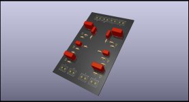
I didn't give up (yet). i made a new design. It is a single channel for now. I will add the second channel later. I still have to figure out how to accurately mirror a layout in KiCad. Will have to do that manually i think. I also integrated the PSU on the same board. Not sure about the ground concept. But should be good as a starting point. Also i decided on a second order filter. I will leave the 2SK170 because i have 6 of them here and i want to use them. If i had more i would change the bias circuit. So for now this is a voltage divider bias. It's basically the exact same buffers i built a decade ago and which never made any problems and sounds really good. I would appreciate if someone could sanitize what i have done here.
Attachments
Thank you!
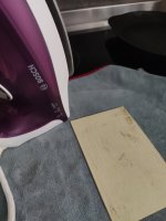
I'm using a SN97CU3 soldering paste that is normally used to solder copper tubes. I'ts simply pasted thick on the tracks and then i bake it in an oven at around 160°C until the paste appears to be dry. Then you can rub that stuff off with some luke warm water.
Here's a link to the paste.
https://www.conrad.de/de/p/felder-loettechnik-sn97cu3-lotpaste-inhalt-250-g-2226426.html
Only use electronic solder for PCBs, plumbing solder usually has agressive acid fluxes that will rot a PCB's thin traces very easily over time. (The acid permeates the fibreglass and leaches back later).
The usable lead-free electronic solder is 95% tin, 4% silver, 0.5% copper, which is a eutectic (important for hand soldering). Chipquik do a large range of pastes for electronics.
The usable lead-free electronic solder is 95% tin, 4% silver, 0.5% copper, which is a eutectic (important for hand soldering). Chipquik do a large range of pastes for electronics.
I'm using this method for 30 years now and never had any problems. My father used it for additional 20 years before me and his PCBs show no sign of what you describe. I believe you, but i guess the issue you describe is more of a hypothetical nature, or is related to other mixtures of solder pastes.
I also used a similar method. It's probably important to clean all residues from the pcb immedately after tinning.
- Home
- Source & Line
- Analog Line Level
- KiCad files: 'The Vulture' a super simple Jfet buffered XO with PSU