hi:
about +20 years ago there was a series of construction articles in a Japanese magazine "MJ" for a No negative feedback Class A power amp ( both BJT and MOSFET).
No voltage gain, just a huge current buffer.
I built the BJT one. I have the construction article somewhere.
I was curious if anyone else has built one or would be willing to comment on the design if I posted the circuits ?
Also there was a No NFB class A pre-amp using a single power JFET. Similar request.
P
Sorry for the poor pdf. My scanner ends up tilting the pages. I can do a better job when I go into the office next week.
I think there was an update for the bias scheme but I didn't find it just now.
I built the one on page 2 of the file Class A NFB_2.pdf
I made copies of other MJ articles while I was in Japan a long time ago. Many tube amps too.
P
I think there was an update for the bias scheme but I didn't find it just now.
I built the one on page 2 of the file Class A NFB_2.pdf
I made copies of other MJ articles while I was in Japan a long time ago. Many tube amps too.
P
Attachments
I ran across the articles (japanese), and found these striking circuit diagrams.
What is the use of connection '5' ("TP") in MosFet_NFB_1.jpg?
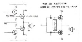
How much 'NO-NFB' is valid in MosFet_NFB_2_no-nfb.jpg?
How much 'NO-NFB' is valid in MosFet_NFB_2_no-no-nfb.jpg?
What is the use of connection '5' ("TP") in MosFet_NFB_1.jpg?
How much 'NO-NFB' is valid in MosFet_NFB_2_no-nfb.jpg?
How much 'NO-NFB' is valid in MosFet_NFB_2_no-no-nfb.jpg?
Attachments
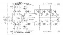
I didn't build the circuit in MosFet_NFB_1.jpg.
Typically "TP" means Test Point.
If the front end( voltage gain) section of the amp was used by itself TP would be the output.When I looked at the PWB and the wiring diagrams in the article, it seems that TP is not connected.
P
Typically "TP" means Test Point.
If the front end( voltage gain) section of the amp was used by itself TP would be the output.When I looked at the PWB and the wiring diagrams in the article, it seems that TP is not connected.
P
Sorry, I don't understand your other questions:
How much 'NO-NFB' is valid in MosFet_NFB_2_no-nfb.jpg?
How much 'NO-NFB' is valid in MosFet_NFB_2_no-no-nfb.jpg?
There is no NFB in the output stage. Only uses NFB in the voltage gain stage. The output stage is a huge buffer so any weird speaker and speaker cable impedance swings won't affect the NFB in the voltage gain stage.
P
I know that.Typically "TP" means Test Point.
he front stage (within the dotted line) is a regular NFB circuit. The output stage with the mosfet's are not linear.If the front end( voltage gain) section of the amp was used by itself TP would be the output.When I looked at the PWB and the wiring diagrams in the article, it seems that TP is not connected.
P
"How much 'NO-NFB' is valid in MosFet_NFB_2_no-nfb.jpg?"
As said in #7, only the output stage is without NFB. It's a firm claim to name it a NFB-less amplifier.
"How much 'NO-NFB' is valid in MosFet_NFB_2_no-no-nfb.jpg?"
It is a regular amplifier with overal NFB.
"...so any weird speaker and speaker cable impedance swings won't affect the NFB in the voltage gain stage."
That's what zillion amps suffer from?
In general, a " "MJ" for a No negative feedback Class A power amp ( both BJT and MOSFET)." is quite a big claim in my opinion.
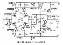
I as I wrote before I didn't build the one with a generic pre-amp block. I built the other article's BJT Class A amp with no negative feedback.
I built a single power JFET(? may be it was mosfet) class A pre-amp. I will keep looking as I know I have the schematic somewhere. I think it ran about 70W of dissipation.
I built a single power JFET(? may be it was mosfet) class A pre-amp. I will keep looking as I know I have the schematic somewhere. I think it ran about 70W of dissipation.
![DSC_2836[1].JPG](/community/data/attachments/1058/1058773-8fb00dffdb3dc8e6c55b76c475a6a44d.jpg?hash=j7AN_9s9yO)
My library is not indexed either, so delays are ok.
That's a no-nfb circuit proper (safe the source-degeneration). The Pass-section on this site is a reference for those circuit's, and they work well and (seem to) sound very good too!
That's a no-nfb circuit proper (safe the source-degeneration). The Pass-section on this site is a reference for those circuit's, and they work well and (seem to) sound very good too!
Clarification, I used the simple Class A MOSFET pre-amp to drive the BJT buffer. Both the preamp and power amp do not have NFB.
P
P
Ah, now I get it: you used the circuit of #10 as a non-feedback amplifier and a non-feedback BJT buffer as a current amplifier.
That's ok. (Safe the local source degeneration feedback in the mosfet amplifier).
Do you have a comparable sketch of this BJT buffer available?
That's ok. (Safe the local source degeneration feedback in the mosfet amplifier).
Do you have a comparable sketch of this BJT buffer available?
#10 The bias scheme is incorrect. There is nfb for current.
Buffer is 99% nfb voltage🙂
Buffer is 99% nfb voltage🙂
Last edited:
- Home
- Amplifiers
- Solid State
- just curious about a MJ class A amp circuit?