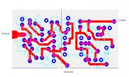
First I should start off by saying - I know this circuit is very sensitive to layout and I pretty much went at it with total disregard for adhering to any specific layout rules(because I designed it before I read anything -.-). However the goal was to keep it relatively compact, so all traces are quite short. The PCB is double sided so the topside is used for ground.
What I am about to say may be complete drivel and I am sure someone will enlighten me if it is. I am assuming, that even if the circuit layout is 'bad' it will still work, even if the max potential of the design isn’t realised.
What I have built is electrically sound, in that all the components connect to all the right places. At least I 'think' it is, I checked the PCB layout against ALWs circuit 3-4 times before etching and then, having constructed the thing, probably agonized over it half a dozen times more – I can see nothing wrong.
FWIW there are 4 regs powering a DAC, running at +12 +5 +3.3 and -12V. From what I gather, as this is using the same ground plane, the '0v' sense points are basically not used and all the ground points are connected to the ground plane.
I have designed the PCB so that there are separate 'islands' for different grounds. One for power ground, one small one for digital ground and then another for analogue ground. Essentially all the ground points (on the ALW diagram) NOT listed as the '0v' sense point are soldered directly to power ground. Then all the points listed as 0v sense are soldered onto the ground plane the regulator circuit will be powering. The idea here, that I could use the sensing function of the circuit and take wires from the different ground planes back to the star ground of the case. The different ground areas are close together so they can all be connected together without any hassle. From what I understand this is not quite how the circuit works, so the analogue and digital grounds were connected to power ground.
I am using a 2.5V reference (LM336Z-2.5) with a 3.3v zener 1N5333B in all the circuits. There was some confusion in the ALW pdf file where the parts list and schematics didn't match up, I have however tried using a 1N5342 6.8v zener, but not a high voltage reference. Regardless it seems the 3.3 and 5v versions are supposed to work from a 2.5v reference and a 3.3v zener.
The resistors used for setting output voltage were all calculated with the standard formula listed in the datasheet for the ALW regs.
Bottom line is once built they do not work.
My first question (I am well aware I have not listed any details on 'what' doesn't work, yet 😉) is a very simple one and could explain an awful lot, do the pinouts vary on the transistors? I have read somewhere that a few EU and US transistors have different pin outs. Something as simple as this would go a long way to explain why I am not having any success. However digging through data sheets seems to suggest this is not the case.
I have tried the AD817 and AD797 in the circuit with different results for each one. I had to buy the 817s from a different place then the rest of the components, because of this I had the regs built but no 817s, so I used the 797s in the meantime.
This is all being tested with a bench power supply with 2.5v reference and 3.3v zeners.
If I power up slowly, no current limiting but I increase the voltage myself, I get to around 6.4V then the LEDs turns on, dimly, its not anywhere near what you’d call bright, should it be bright? At this point I can slowly increase the output voltage up to 18v, the max of the unit, and all the LEDS stay on. When measured the output voltage is stuck on ~3.4v. If I measure the output voltage as I power on, it increases with the input voltage then as soon as the LED turns on, it stops getting any higher. The –ve regulator measures –3.8volts. All the positives give the same output.
The pre regulator does exactly what it should be doing however and its output measures 2.5v above the regulators.
If I place this 3.4v under load (100mA) the pre reg heats up, and the D44 tranny gets ever so slightly warmer. The output voltage falls by about 0.1v.
Now, if I power the units on quickly. As in no current limiting, with the power supply set to its max voltage. Upon power up, the LEDs will flash on and then off again and the output voltage stays ~2.25V above the input voltage. So with 18v on the input of the prereg, the output measures 15.75v. When the input voltage falls the difference between input and output drops slightly too, down to about 2v.
After the LEDS have flashed on and off - if I now lower the input voltage, when I reach 6v the LEDS will flash once more, very faintly this time though, less then before. If I now increase the input voltage, after this second flash, the LEDS will come on and the aforementioned 3.4v on the output will come back.
The negative version works in exactly the same way, but when powered on quickly the LED comes on and just stays on, so works in the same way as being slowly powered up.
Now – with the AD817 in place I get different results, whether this means the 797 was unstable I have no idea, it does not get warm under any circumstance, and none of the opamps have been destroyed in use.
With the AD817 in the 12V reg, when powered on slowly the LED wont illuminate at all. If turned on quickly it will flash briefly then go out. If the input voltage is lowered down it will not blink, as in the case of the 797.
In the +5 and 3.3v regulators, upon fast power up the LEDS flash on and off, but its slower, they start off dim and glow brightly before going out, this takes about 1 second.
I have tried replacing all the components in one reg and it made no difference.
I have tried all the various combinations of resistors used to bias the reference + the one closely linked to it, with very little change. Currently I am using 499R for the resistor connected to +ve opamp input and the reference, and 249R between the reference and the output.
If it turns out my PCB is the main cause of this, then I have no issues with a redesign + remake as I have all the stuff to do that on hand. I would just expect them to work, perhaps not with the same specification as ALWs board design, but at least get all the correct voltages.
I also have two smaller boards made to power active crossovers. I could simply wire up one of these and see how that fairs, in isolation without being connected to anything at all.
If anyone can think of anything helpful that could help solve this, I would greatly appreciate it.
Thanks in Advance,
Matt.
P.S. I have read through a lot of the information on Walt Jungs website, relating to super regs, but I find it very hard going as I unfortunately live with chronic fatigue so cannot process much at any one time.
The answer is yes, ....occationally. Checking with datasheets is essential if you make a board. If you aren't 100% sure why don't you make yourself sure?5th element said:
My first question (I am well aware I have not listed any details on 'what' doesn't work, yet 😉) is a very simple one and could explain an awful lot, do the pinouts vary on the transistors? I have read somewhere that a few EU and US transistors have different pin outs. Something as simple as this would go a long way to explain why I am not having any success. However digging through data sheets seems to suggest this is not the case.
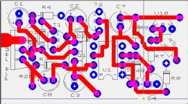
Bonsai said:Post a picture and your layout - that way we can all look at it and offer some advice.
OK here is a picture of the schematic for a +ve version.
Ignore the polarity of the capacitors and diodes as they were not set when designing the PCB, as I always build things with the component data sheets and schematics in front of me.
The first diode on the left is the LED. I am aware that the orientation of the voltage reference is incorrect, its a diode remember, but its a transistor case, so I thought I'd just mention it. All the transistors have been installed relative to how the PCB is lay out.
Also I have removed the ground plane to make viewing it easier, just assume that if there is anything unconnected, it probably goes to ground.
Many thanks again, I know looking over someone elses PCB can be a headache, but I'd really like to get to the bottom of why this isn't working.
Matt
Attachments
Check the Vbe's of the current source/sink transistors. If they are not something like +/- 0.65V, check correct pinout in datasheets.
AndrewT said:Hi,
could you post the schematic that goes with the component naming?
I dont really understand what you are asking here, as when I make PCBs the CAD program doesnt name anything with any relavence to the schematic. If you wish I can rename all the components with regards to a schematic.
The Schematic I used is the one from ALW's website. BrianGT also drew up a schematic too, which is here
http://brian.prohosting.com/reg/jung-schematic.gif
his final schematic seemed to gain acceptance and indeed it does seem to mirror ALW's.
And the pinout of the all transistors has been checked several times against the datasheets, so as far as I can see everything should be right there.
peranders said:Pin 7 of the opamp, can you tell me where you have connected it on the pcb?
The trace beneath the pin? The output.
It's very common5th element said:I dont really understand what you are asking here, as when I make PCBs the CAD program doesnt name anything with any relavence to the schematic. If you wish I can rename all the components with regards to a schematic.
 that the parts are named R1, R2, R3 etc and also in the schematic. Every pcb cad program can rename the parts.
It could be a help that you take a picture so we can see how you ave mounted the parts.
peranders said:
It's very common
It could be a help that you take a picture so we can see how you ave mounted the parts.
Noted^^ I will get on it.
When using AD797 - ie when the LEDS light up as in post one - Vbe on T1 measures 0.62V and T2 measures exactly the same, so all's well there.
With an AD817 in place - T1 Measures 0.66V and T2 measures 0.425V. So not so good.
Incidentally - The regulated voltage with AD797 is always 3.4V as explained in the original post. With an AD817 in place it measures say 15V (it depends on input voltage, but this isnt important for now), with NO opamp in place at all, you get the same voltage. So with no opamp or the AD817 you get the same on the output, its as if the opamp isnt even there. As I understand it, its the opamp thats the controlling device here, and regulates the output voltage. I dont know what this means, but I thought it might be useful.
I had read somewhere also, that on turn on there is a very short time where the voltage created between two components (voltage reference and 3.3/6.8v zener? I dont remember now) allows for the opamp to power on before the rest of the circuit? Thus allowing regulation to take place? Maybe the opamp isnt turning on in time, or more the voltage isn't sufficient to turn it on. And the fact the -ve output voltage is 3.8V instead of 3.4, perhaps something internal is working at a higher voltage, so on a very quick turn on, it still functions, as the instantaneous voltage to the opamp is sufficient to turn it on.
Say there is a period of overlap. The circuit for some reason is regulating at 3.4v. THe AD797 is comfortable working at 2.5v, the rest of the circuit turns on at 3.0v. But the AD797 needs a little bit of time at such a low voltage to work correctly. So when I turn up the wick slowly it gives it time to switch on. But when I power up quickly the regulator switches on before the opamp has stabilized and thus no regulation takes place. Maybe the -ve voltage one is working with slightly different tolerances/NPN vs PNP differences, so the voltage supplied to the opamp at turn on is a bit higher, allowing it to ping on.
I do have OPA627 TL071 and AD8610 I can try too, if you think this would perhaps shed some more light.
Meh guess work from someone uneducated in this field -.-
Sounds like oscillation to me.
What are you connecting this circuit to (i.e. what's your load)?
do you have any additional output capacittance connected to it?
What are you connecting this circuit to (i.e. what's your load)?
do you have any additional output capacittance connected to it?
Do you have any bypassing caps between the power pins of the op amp? Try a 0.1u or 0.01u directly across pins 7 and 4. Also double check your resistor values. You may have the components connected properly but that doesn't ensure they're the proper values. You could also try lowering the values of R2 and R3 to something like 499 or 249 (since you already have those handy).
This is actually not a good idea in this design!BWRX said:Do you have any bypassing caps between the power pins of the op amp? Try a 0.1u or 0.01u directly across pins 7 and 4.
why not?Originally posted by BWRX
Do you have any bypassing caps between the power pins of the op amp? Try a 0.1u or 0.01u directly across pins 7 and 4.
Originally posted by peranders
This is actually not a good idea in this design!
The opamp is making high speed corrections to allow the pass transistor to react to downstream current demand changes.
Just like any opamp, it should perform better when it's supplies suffer from smaller glitches.
And these glitches will similarly be attenuated before they ripple through to the other (sensitive) components.
Bonsai said:Sounds like oscillation to me.
What are you connecting this circuit to (i.e. what's your load)?
do you have any additional output capacittance connected to it?
The capacitor on the output isnt in place, as advised by ALW in his design papers. The circuits are connected up to a DAC. The 3.3 version, at the chip end has a 0.1uF and a 10uf cap. The 5V connects to a variety of caps around power pins near the DAC chip, nothing of large value though. Then the + and -12V regs are connected to 6 opamps each with 0.1uF bypassing near each power pin.
BWRX said:Do you have any bypassing caps between the power pins of the op amp? Try a 0.1u or 0.01u directly across pins 7 and 4. Also double check your resistor values. You may have the components connected properly but that doesn't ensure they're the proper values. You could also try lowering the values of R2 and R3 to something like 499 or 249 (since you already have those handy).
Yes I have used bypassing on the opamp with no difference in performance. The resistor values have been checked many many times, have already tried 449R for R2 and R3.
My main concern was with the layout, does this look alright then?
Hi 5th element,
check on this post i have many problem with same PS. you have diodes on pin 2 and 3, i removed these diodes and all is OK.
http://www.diyaudio.com/forums/showthread.php?threadid=78162&perpage=10&pagenumber=3
Maxpou
check on this post i have many problem with same PS. you have diodes on pin 2 and 3, i removed these diodes and all is OK.
http://www.diyaudio.com/forums/showthread.php?threadid=78162&perpage=10&pagenumber=3
Maxpou
- Status
- Not open for further replies.
- Home
- Amplifiers
- Power Supplies
- Jung/ALW reg issues.