Scott,
Did you mean 2SJ74V/2SK170V or 2SK246BL/2SJ103BL?
The datasheet of 2SK246 and 2SJ103 don't have V grade, BL is the highest. See attachments.
Thanks,
Did you mean 2SJ74V/2SK170V or 2SK246BL/2SJ103BL?
The datasheet of 2SK246 and 2SJ103 don't have V grade, BL is the highest. See attachments.
Thanks,
Attachments
Last edited:
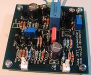
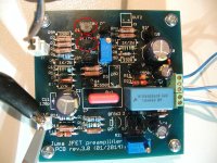
Finally also my boards arrived. Thanks Prasimix!
Using single channel PCBs I will go for a barebones J74/K170 version (without buffers), with reduced gain, and configured for balanced operation.
Now I just have to work out exactly how🙄
Using single channel PCBs I will go for a barebones J74/K170 version (without buffers), with reduced gain, and configured for balanced operation.
Now I just have to work out exactly how🙄
Finally also my boards arrived. Thanks Prasimix!
Using single channel PCBs I will go for a barebones J74/K170 version (without buffers), with reduced gain, and configured for balanced operation.
Now I just have to work out exactly how🙄
If you'd like to remove buffer don't forget to add JP1.
Attachments
Scott,
Did you mean 2SJ74V/2SK170V or 2SK246BL/2SJ103BL?
The datasheet of 2SK246 and 2SJ103 don't have V grade, BL is the highest. See attachments.
Thanks,
pchw:
Interesting, and this shows my ignorance. I thought the "V" at the end of 2SJ74V and 2SK170V reflected the grade. I apologize for any confusion, but what I have purchased (and will eventually receive) was listed as 8 sets of matched "2SJ74V/2SK170V" on a Japanese auction site. There was a lot of other text as well which was even less comprehensible to me.
Regards,
Scott
Got my board. Everything arrived in perfect condition. The PCB looks great!
Thank you for organizing this GB.
Regards,
David
Thank you for organizing this GB.
Regards,
David
Ok - I have a few more questions. As some of them are somewhat "board-specific" I will asked them in this thread:
Q1: Will thermal coupling of J74/K170 make any difference? I guess there might also be a benefit of thermally coupling the BC550/BC560 and the J310s, even if this will not be possible with the current layout. Any comment are highly appreciated.
Q2: The Q1A/R4A/R4B creates a CCS alternative to R4. Using the simple solution (only R4) the current will vary with rail voltage, while it will not do so as much with the CCS in place. Correct?
Q3: Configured as a phase splitter the circuit may be used to convert a single ended line signal to a balanced one (SE-> Bal). Correct?
Q3A: If used as a SE-> Bal converter I can omit the buffer when used in front of a balanced pre with 100K input impedance. Correct?
Q3B: If used as a SE-> Bal converter I may even also omit the cascode and lower the rail voltage. Correct?
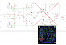
I finished single channel version with 2SK246/2SJ103 jfets in input stage. Instead of 1K/2W resistor I tried to use J310 (see attached schematic).
Please note that 2SK246/2SJ103 are rotated 180 degree (marked red on first picture)
A few words about fet matching. I bought from pacificsemi.com 4 pair of 2SK246/2SJ103 and succeed to match two pair well within 0.1mA (@ Vgs=10V). I used 7.10mA 2SK246 and 7.11mA 2SJ103. From Farnell comes 8 pairs of J310 and I found only one pair within 1mA (31.5mA and 31.6mA @Vgs=10V) what is still not bad since this one is really cheap.
Attachments
Last edited:
Ok - I have a few more questions. As some of them are somewhat "board-specific" I will asked them in this thread:
Q1: Will thermal coupling of J74/K170 make any difference? I guess there might also be a benefit of thermally coupling the BC550/BC560 and the J310s, even if this will not be possible with the current layout. Any comment are highly appreciated.
Q2: The Q1A/R4A/R4B creates a CCS alternative to R4. Using the simple solution (only R4) the current will vary with rail voltage, while it will not do so as much with the CCS in place. Correct?
Q3: Configured as a phase splitter the circuit may be used to convert a single ended line signal to a balanced one (SE-> Bal). Correct?
Q3A: If used as a SE-> Bal converter I can omit the buffer when used in front of a balanced pre with 100K input impedance. Correct?
Q3B: If used as a SE-> Bal converter I may even also omit the cascode and lower the rail voltage. Correct?
Q1: Don't know.
Q2: Yes, I tested that on single channel PCB (see previous post).
Q3: I hope so 🙂
Q3A: Yes
Q3B: Yes, and if you still wants to use 5-pole power connector you can add two jumper to bring 24V to 33V rail (marked red on picture). Of course both 33V sections on PS PCB are not populated in that case.
Attachments

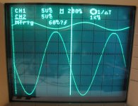
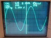
Small correction: on picture of 1kHz signal posted in #188 you can see clipping on positive half what is caused because I forgot to solder on leg of R18 🙂 That caused huge DC offset on buffer output (approx. 5V).
Here is a new nice picture for the same input signal.
Here is a new nice picture for the same input signal.
Attachments
Folks:
A slightly updated BOM for the North American community.
Regards,
Scott
Be prepared to use 22R instead of 47R for R21 and R47 if you are not in position to match BF862 what is in fact realistic scenario since it's not easy at all to play with so small devices (see post #364).
I start to fill the board today and have some questions:
In your BOM and schematic R2 R3 R29 and R30 are 330R however in the PCB it read 470R. I believe 330R is correct, right?
There is no R14 and R25 (both are 27R) and C11 and C30 in 2sk246/103 version right?
In the main thread post #114 juma suggested that for k170/j47 version, changing R9 and R37 can change the gain. Is this the same for 2sk246/103 version? If I change R9 and R37 to a lower value, I can reduce gain of the circuit?
Thank
Please note that values printed on PCBs are for 2SK170/2SJ47 version. Therefore R2, R3, R29 and R30 are 470R. Use 330R if you choose 2SK246/2SJ103 version.I start to fill the board today and have some questions:
In your BOM and schematic R2 R3 R29 and R30 are 330R however in the PCB it read 470R. I believe 330R is correct, right?
Right, omit that RC filter for 2SK246/2SJ103 version.There is no R14 and R25 (both are 27R) and C11 and C30 in 2sk246/103 version right?
In the main thread post #114 juma suggested that for k170/j47 version, changing R9 and R37 can change the gain. Is this the same for 2sk246/103 version? If I change R9 and R37 to a lower value, I can reduce gain of the circuit?
Thank
Maybe you should ask this question Juma directly on main thread?
You're right. Even with 300mA load there is minor voltage drop (cca 1.5V) what is far beyond 18VAC. In that case suggested 18VAC pcb transformers in the BOM list are not appropriate. I'll try to get one with 2x15VAC.
Just to inform you that I tried to use Block 2x15VAC FL10/15 PCB transformer (Farnell no. 1131490). Unfortunately that didn't make any change, on 33V rails I have more than 50V and 7924 reg cannot work. Don't know what to suggest for transformer and what is in the BOM is not something what I can recommend.
look at leerlauf spannung/ no load voltage factor
http://docs-europe.electrocomponents.com/webdocs/04f3/0900766b804f3ba4.pdf
smallest 2VA is 1.35 and biggest 52VA is 1.12
btw, would it help to use a drain resistor ?
http://docs-europe.electrocomponents.com/webdocs/04f3/0900766b804f3ba4.pdf
smallest 2VA is 1.35 and biggest 52VA is 1.12
btw, would it help to use a drain resistor ?
look at leerlauf spannung/ no load voltage factor
http://docs-europe.electrocomponents.com/webdocs/04f3/0900766b804f3ba4.pdf
smallest 2VA is 1.35 and biggest 52VA is 1.12
btw, would it help to use a drain resistor ?
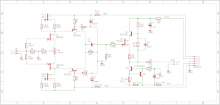
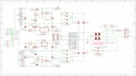
I tried to add actually two resistor to came down to +/-24 and +/-33V with 2x15V 10VA transformer. Check schematic below.
Dissipation of 2K resistor is around 500mW, and 240R around 1.3W.
Attachments
- Status
- Not open for further replies.
- Home
- Group Buys
- Juma's LSK Preamp - through hole version