Ouput Trannies
Hello Edmond
You say
>>4- How large is Iq of the output trannies? In my sim I've fixed it at 1.6mA by taking these trannies 20 times as large. To what extent is this correct?
To make a transistor 20 times as large, how do this in microcap is it the same as increasing the value in the individual transistor to 20.
I also notice you connect C2 ( 50pf) to negative supply is that detail in the AES paper, it always gets me how they show cap to gound in internal circuit detail when there is no ground pin on most opamps.
Regards
Arthur
Re: Ouput Trannies
Hi Arthur,
That's right, VALUE=20
I guess the sales department made objections as an extra pin is way too expensive. 😉
Also separate supply pins for the front end and OPS would make that chip more versatile (think of an Alexander amp, for example).
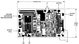
Notice that the chip itself seems to have separate connections though (see pic)
Regards,
Edmond.
PS: How about the MOSFETs?
PHEONIX said:Hello Edmond
You say
>>4- How large is Iq of the output trannies? In my sim I've fixed it at 1.6mA by taking these trannies 20 times as large. To what extent is this correct?
To make a transistor 20 times as large, how do this in microcap is it the same as increasing the value in the individual transistor to 20.
Hi Arthur,
That's right, VALUE=20
I also notice you connect C2 ( 50pf) to negative supply is that detail in the AES paper, it always gets me how they show cap to gound in internal circuit detail when there is no ground pin on most opamps.
Regards
Arthur
I guess the sales department made objections as an extra pin is way too expensive. 😉
Also separate supply pins for the front end and OPS would make that chip more versatile (think of an Alexander amp, for example).
Notice that the chip itself seems to have separate connections though (see pic)
Regards,
Edmond.
PS: How about the MOSFETs?
Attachments
Re: Ouput Trannies
In IC technologies, "ground" is the silicon wafer backside (aka "substrate"). In common bipolar technologies, from a DC perspective, the substrate should always be at the most negative potential (usually the negative rail). For all AC purposes this is electrical ground, so in electrical schematics sometimes substrate/isolation tower capacitors are shown as connected to the ground.
This would explain, for example, why the TO220 LM337 (negative regulator) has the input pin as "bipolar collector". The input is the most negative potential, is connected to the substrate, which in turn is soldered to the TO220 copper plate. In LM317 (positive regulator) the most negative potential is the ground, therefore the TO220 plate ("bipolar collector") can be connected to the ground, a heatsink insulator is not required.
PHEONIX said:
I also notice you connect C2 ( 50pf) to negative supply is that detail in the AES paper, it always gets me how they show cap to gound in internal circuit detail when there is no ground pin on most opamps.
In IC technologies, "ground" is the silicon wafer backside (aka "substrate"). In common bipolar technologies, from a DC perspective, the substrate should always be at the most negative potential (usually the negative rail). For all AC purposes this is electrical ground, so in electrical schematics sometimes substrate/isolation tower capacitors are shown as connected to the ground.
This would explain, for example, why the TO220 LM337 (negative regulator) has the input pin as "bipolar collector". The input is the most negative potential, is connected to the substrate, which in turn is soldered to the TO220 copper plate. In LM317 (positive regulator) the most negative potential is the ground, therefore the TO220 plate ("bipolar collector") can be connected to the ground, a heatsink insulator is not required.
How sensitive are the values of C1, C2 & C5 to the performance and stability of the 797 discrete amp, particularly as closed loop gain is adjusted?
Re: Ad797
1 - The lower number is correct, the other was probably a mistake (1.8+.5 instead of .9+.5 ??) don't remember.
2 - The supply current would have increased, 400uA was enough.
3 - This gets tricky, at high frequencies it acts like degeneration in an integrating VAS (sort of) making a right plane zero where you don't want it. The compensation details >50MHz are too involved and entail actual models. As an asside the need for snubbers at low closed loop gains is, as I mentioned before, probably due to the strange input devices (that violate design rules and were not modeled).
4 - 500uA
Edmond Stuart said:
Hi Scott,
With above values for the current sources, the sim runs much better now. No issues with Q64 any longer. Thanks!
If G=10, RL=1k, Vo=3Vrms and Iq of Q22 & Q23=1.6mA, then THD20=0.6ppm (mostly H2). That's great. (BTW John, H7 = 1.8ppb)
Nevertheless, I still have a few questions:
1- Somewhere else in your paper R1 and R2 are depicted as 2.3mA current sources (I2=I3 on page 4 and fig. 1 on page 9), while according to the sim these currents are only 1.43mA. So why this discrepancy and which is the correct value?
2- Why is the current through the folded cascoce so much lower (0.52mA) than Ic of Q5 & Q6 (0.92mA)? Wouldn't it be more appropriate to make them equal?
3- Why has R9 such a low value? If increased to say 180 Ohms the Vce balance between Q16 and Q17 is better.
4- How large is Iq of the output trannies? In my sim I've fixed it at 1.6mA by taking these trannies 20 times as large. To what extent is this correct?
Regards,
Edmond.
1 - The lower number is correct, the other was probably a mistake (1.8+.5 instead of .9+.5 ??) don't remember.
2 - The supply current would have increased, 400uA was enough.
3 - This gets tricky, at high frequencies it acts like degeneration in an integrating VAS (sort of) making a right plane zero where you don't want it. The compensation details >50MHz are too involved and entail actual models. As an asside the need for snubbers at low closed loop gains is, as I mentioned before, probably due to the strange input devices (that violate design rules and were not modeled).
4 - 500uA
Gentlemen, I posted the beta graph from our MAT02 data sheet a two weeks ago, it is essentially flat.
I am shocked and dismayed that this AD797 model has been made without knowing the exact amount of current allowed in each stage. It is virtually pointless as a practical example, although it might be useful as a learning tool. Now, this really belongs in the SIM thread and not here.
Edmond, this is an idealized model, and not a REAL model. It is not going to give REAL measurement results. Please get REAL, yourself. I appreciate Scott's forthright honesty on this, as I have always presumed .5ma output bias. THAT IS MY PROBLEM with the AD797! from the get-go. MY output circuits use 30-50ma. I don't have to address the same problem. Does everyone understand this?
john curl said:THAT IS MY PROBLEM with the AD797! from the get-go. MY output circuits use 30-50ma. I don't have to address the same problem. Does everyone understand this?
Nobody understands what your problem is and what your expectations are. If you don't like it, don't use it. Trying to mess with the 797 (or any other IC, from this perspective) will only worsen the performances you may get out of the box.
It would be wonderful, IF the REAL AD797 had 2ma of standing output current, then it could drive its own feedback loop in class A mode, in general
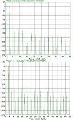
Here's my results John with (on top) a 10ma current source out of the output and below normal. Not much 7th in either case. 30dB gain with 300 Ohm feedback. Our simulator allows you to lockstep time and amplitude which is about 300dB dynamic range for the FFT probably enough. The class A current just keeps making it better there was no null point, except on the 15th harmonic for some reason. At -180dB the results are just numbers.
Another thing to think about, all op-amps have current limit sense resistors made out of very nasty diffusions (usually), high TC non-linear. They're right there in series with the output.
Another thing to think about, all op-amps have current limit sense resistors made out of very nasty diffusions (usually), high TC non-linear. They're right there in series with the output.
Attachments
Hey Scott,
Re NL silicon and previous discussions about DA, how would you describe the on-chip capacitors - like Cc?
Brian
Re NL silicon and previous discussions about DA, how would you describe the on-chip capacitors - like Cc?
Brian
dimitri said:
I believe that ad797 was fabricated with vertical pnp and npn in dielectrically isolated pockets, like US Pat 4665425. I need to have a look in my books for the parameters.
No that's a flavor of Harris DI I think, this is on a junction isolated 36V process now denigrated in favor of SOI (silicon on insolator) processes. JI has all the fun of designing around latch-ups due to unwanted parasitic devices.
traderbam said:Hey Scott,
Re NL silicon and previous discussions about DA, how would you describe the on-chip capacitors - like Cc?
Brian
Pretty good, we once made a sample and hold with an internal 100pF capacitor and a pin to let the user increase it. The 1-2pF leadframe parasitic had more DA than the on chip cap. Had the engineer pounding his head on the bench trying to figure it out too.
Re: Re: AD797, Iq output stage
Hi Scott,
That low? Who has decided that, one of the marketing people?
Admittedly, with Cn installed, the performance isn't much affected by such a low Iq. Without Cn however, much better results would be obtained if Iq was chosen a bit higher. Of course, at the expense of a higher supply current, but who cares? Those who are interested in ultra low noise and distortion, normally don't care about a bit more current (from 8.2 to 10mA or so).
Regards,
Edmond.
PS: I'm away for 9 days. Going to Crete.
scott wurcer said:[snip]
4 - 500uA
Hi Scott,
That low?
Who has decided that, one of the marketing people?Admittedly, with Cn installed, the performance isn't much affected by such a low Iq. Without Cn however, much better results would be obtained if Iq was chosen a bit higher. Of course, at the expense of a higher supply current, but who cares? Those who are interested in ultra low noise and distortion, normally don't care about a bit more current (from 8.2 to 10mA or so).
Regards,
Edmond.
PS: I'm away for 9 days. Going to Crete.
John, the output devices are 16, 11 X 100 micron stripes each. I plotted beta using the simulator and found nothing interesting, it decreases slowly from 1uA Ic to 100mA Ic from 180 to about 90 with no peak. I could never find a Gummel plot (all the folks have retired by now). I'm sure this helps. 🙂
It's a triple bootstrapped darlington so the circuit never "sees" the beta of the output devices under normal loads.
It's a triple bootstrapped darlington so the circuit never "sees" the beta of the output devices under normal loads.
Don't feel too bad, Gummel-Poon is now second rate.😉 It usually is more linear than GP gives you, go figure!
Thanks for the input, Scott.
The purpose of this questioning is not so much for Scott, but ultimately to others, who think that a follower is a follower, and forgetting that it is really a beta multiplier. It has to to do with the relatively hi Z drive impedance and the relatively low output load. Scott, can you tell us the drive impedance of the input stage, within an order of magnitude?
- Status
- Not open for further replies.
- Home
- Amplifiers
- Solid State
- John Curl's Blowtorch preamplifier