http://www.eecs.umich.edu/~singh/bk7ch08.pdf
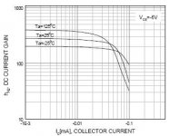
LOW INJECTION REGIME: Current gain is small because of non-ideal generationrecombination current.
HIGH INJECTION REGIME: Current gain drops because the effective base width is pushed out into the collector + carriers (e-h) recombine due to Auger effect.
Re: http://www.eecs.umich.edu/~singh/bk7ch08.pdf
It happens me to know pretty well what you are quoting 🙂. It is completely irrelevant in this context, and I suppose you know it. It was an issue 40 years ago, in the uA702 process, where JC's understanding of integrated electronics is still confined.
Therefore, if you want to support JC, you have to find a better way. This one is doomed to fail, for any modern bipolar process, "low injection" is in the uA range and "high injection" is in the hundreds of mA or even amps. In between, beta is constant for all practical purposes.
dimitri said:
Dmitri,
LOW INJECTION REGIME: Current gain is small because of non-ideal generationrecombination current.
HIGH INJECTION REGIME: Current gain drops because the effective base width is pushed out into the collector + carriers (e-h) recombine due to Auger effect.
It happens me to know pretty well what you are quoting 🙂. It is completely irrelevant in this context, and I suppose you know it. It was an issue 40 years ago, in the uA702 process, where JC's understanding of integrated electronics is still confined.
Therefore, if you want to support JC, you have to find a better way. This one is doomed to fail, for any modern bipolar process, "low injection" is in the uA range and "high injection" is in the hundreds of mA or even amps. In between, beta is constant for all practical purposes.
john curl said:Let them live in ignorance, Dimitri!
 You are boring, John. You could consult your associates for a better insult repertoire.
A diffused base, diffused emitter, n-p-n silicon switching transistor has been developed for high-current applications such as switching magnetic memories. The transistor is designed to operate as a switch at the 0.75- ampere level. For a collector current of 0.75 ampere, the large signal current gain is 20 and the saturation voltage drop 4 volts. The breakdown voltages are 75 volts collector-to-base, and 6 volts emitter-to-base. The unit shows fast switching characteristics. The rise, storage, and fall times are each of the order of 0.1 µsec. It has a common emitter unity gain frequency greater than 50 Mc. The transistor employs a localized emitter produced by photoresist techniques and oxide masked diffusion. Lead attachment is accomplished by compression bonding. The silicon wafer is bonded through a molybdenum intermediary to a massive copper stud. The design theory of the device, and the variation of device characteristics with temperature are given. The applicability of this devices to RF amplifier service is also discussed.
dimitri said:
These are current bjts
You are off topic. a) The subject is IC processes, not discrete devices. b) current ranges in the uA are irrelevant here and c) take a look at your own picture. How much can you hope to adjust the collector current? 10mA? for such, beta increases from 85 to 90. Wow, quite a change
The question is not if the beta depends on Ic, it's if this is relevant for any practical purposes, and it is not. You are again misleading and playing dumb - you can do better than that.
Wavebourn said:A diffused base, diffused emitter, n-p-n silicon switching transistor has been developed for high-current applications such as switching magnetic memories. The transistor is designed to operate as a switch at the 0.75- ampere level. For a collector current of 0.75 ampere, the large signal current gain is 20 and the saturation voltage drop 4 volts. The breakdown voltages are 75 volts collector-to-base, and 6 volts emitter-to-base. The unit shows fast switching characteristics. The rise, storage, and fall times are each of the order of 0.1 µsec. It has a common emitter unity gain frequency greater than 50 Mc. The transistor employs a localized emitter produced by photoresist techniques and oxide masked diffusion. Lead attachment is accomplished by compression bonding. The silicon wafer is bonded through a molybdenum intermediary to a massive copper stud. The design theory of the device, and the variation of device characteristics with temperature are given. The applicability of this devices to RF amplifier service is also discussed.
Is this from the 50's? Current integrated devices have Ft in the GHz range 😀syn08 said:
No, it is exactly 1960. I like 4V saturation. And magnetic memory. 😀
The subject is IC processes
I believe that ad797 was fabricated with vertical pnp and npn in dielectrically isolated pockets, like US Pat 4665425. I need to have a look in my books for the parameters.
And you are again trying to play paternal role here - sorry this one has been already taken over.You are again misleading and playing dumb
syn08 said:
Earlier in this thread, Scott mentioned that the process used for the AD797 had fT of ~400 MHz (this is from memory here).
Dimitri, while I appreciate you putting up the beta curves, you did not put a reasonable worst case beta curve for the low current bjt, because you used a pnp rather than an npn. Please note this, because the beta will probably sag at low currents with the complementary npn device.
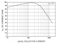
Also, I have here, but can't find it at the moment, a beta curve of an npn output device for a
Raytheon IC, made about 1991. It is here, somewhere, and it does tell the story, if Scott's bjt is no better.
Also, I have here, but can't find it at the moment, a beta curve of an npn output device for a
Raytheon IC, made about 1991. It is here, somewhere, and it does tell the story, if Scott's bjt is no better.

What I feel as a real pain with even small BJTs is that one cannot rely on datasheet curves and parameters. The 'same' part differs depending on manufacturers. Obviously they use different chips for the same part designation. I had a big trouble with BC5XY transistors, hundreds of boards perfect nad then different part manufacturer resulted in the local oscillations I am attaching.
Attachments
Ad797
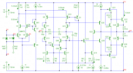
Hi Scott,
With above values for the current sources, the sim runs much better now. No issues with Q64 any longer. Thanks!
If G=10, RL=1k, Vo=3Vrms and Iq of Q22 & Q23=1.6mA, then THD20=0.6ppm (mostly H2). That's great. (BTW John, H7 = 1.8ppb)
Nevertheless, I still have a few questions:
1- Somewhere else in your paper R1 and R2 are depicted as 2.3mA current sources (I2=I3 on page 4 and fig. 1 on page 9), while according to the sim these currents are only 1.43mA. So why this discrepancy and which is the correct value?
2- Why is the current through the folded cascoce so much lower (0.52mA) than Ic of Q5 & Q6 (0.92mA)? Wouldn't it be more appropriate to make them equal?
3- Why has R9 such a low value? If increased to say 180 Ohms the Vce balance between Q16 and Q17 is better.
4- How large is Iq of the output trannies? In my sim I've fixed it at 1.6mA by taking these trannies 20 times as large. To what extent is this correct?
Regards,
Edmond.
scott wurcer said:Thanks to a little help I was able to resurrect a complete working sim of the 797
Edmund - these are the values of the currents in your schematic (the published one).
The voltages on the collectors of Q16 and Q17 are (vout = 0) -.580, -.672.
Q61 BTW is part of the Ib comp circuit. You won't be able to get the output stage to
bias right without the correct area ratios, but the front end has so much degeneration
that it should be close.
I1 = 1.84ma ,I2 = .3mA ,I3 = 2.6mA ,I4 = .51mA ,I5 = .49mA ,I6 = .215mA
[snip]
Hi Scott,
With above values for the current sources, the sim runs much better now. No issues with Q64 any longer. Thanks!
If G=10, RL=1k, Vo=3Vrms and Iq of Q22 & Q23=1.6mA, then THD20=0.6ppm (mostly H2). That's great. (BTW John, H7 = 1.8ppb)
Nevertheless, I still have a few questions:
1- Somewhere else in your paper R1 and R2 are depicted as 2.3mA current sources (I2=I3 on page 4 and fig. 1 on page 9), while according to the sim these currents are only 1.43mA. So why this discrepancy and which is the correct value?
2- Why is the current through the folded cascoce so much lower (0.52mA) than Ic of Q5 & Q6 (0.92mA)? Wouldn't it be more appropriate to make them equal?
3- Why has R9 such a low value? If increased to say 180 Ohms the Vce balance between Q16 and Q17 is better.
4- How large is Iq of the output trannies? In my sim I've fixed it at 1.6mA by taking these trannies 20 times as large. To what extent is this correct?
Regards,
Edmond.
Attachments
- Status
- Not open for further replies.
- Home
- Amplifiers
- Solid State
- John Curl's Blowtorch preamplifier