Hi Brian,
Hi Andy,
can you put VCVS instead of Q7 and play with it gain (0.9, 0.99, ...)? It looks like the deviation from unity is a limiting factor for
Wait, wait 🙂, one important follower is omitted 🙂Dimitri's diagram makes more sense to me.
Hi Andy,
can you put VCVS instead of Q7 and play with it gain (0.9, 0.99, ...)? It looks like the deviation from unity is a limiting factor for
loop gain inside the "neutralization loop"
dimitri said:Hi Andy,
can you put VCVS instead of Q7 and play with it gain (0.9, 0.99, ...)? It looks like the deviation from unity is a limiting factor for [loop gain]
Sure. I'm just about to eat dinner, so I'll need a bit of time.
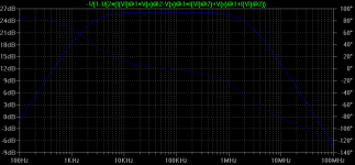
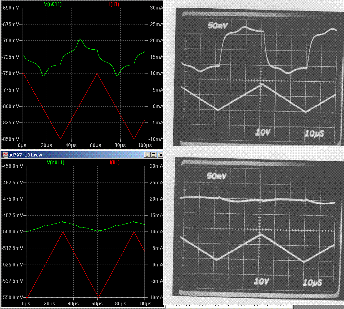
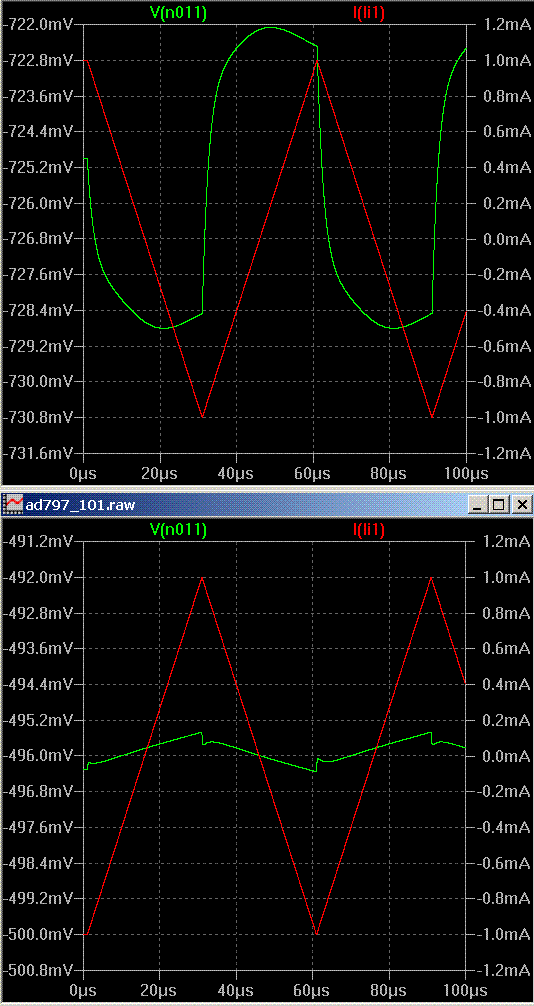
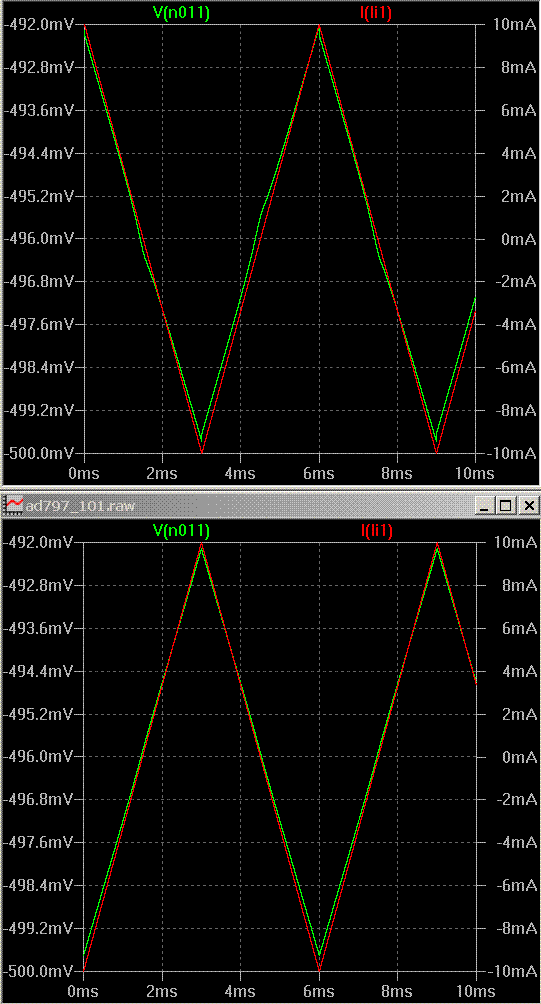
OK, here is a loop gain plot with a VCVS of value 0.9999. Unfortunately, I can't plot a family of curves with the VCVS scale factor as a parameter, because the loop gain calculation itself uses .STEP and the calculation becomes borked when trying to use it in conjunction with other .STEP commands. I've duplicated the bias conditions of using the EF, with the emitters of the current mirror at -2.2 Volts DC.
Anyway, you can see the loop gain is higher, though not exceedingly so. The loop gain is way more broadband now. The interesting thing is that the unity loop gain frequency has gone from about 1.5 MHz to about 45.5 MHz. It's still stable though.
Edit: I can't get this to look like the EF case regardless of VCVS scale factor. This may be because of the output impedance of the EF, which has about 90 uA Ic.
Attachments
traderbam said:I feel an urge to ask you how you distinguish between feedback and "subtractive neutralization" in a mathematical sense. I find textual descriptions are generally hard to interpret without ambiguity. 🙂
This is an interesting question per se; how do you mathematically identify feedback? That is, given a complex function that defines a linear and time invariant causal system how do you decide it originates from a "feedback circuit", e.g. a A/(1+A*B) form can be derived (or any other criteria that defines "feedback circuit"?).
I've said it before - to me, feedback is more like an analysis instrument rather that a circuit topology.
I think that resolving this 'ambiguity' resides in the math, rather than explanations. I recall trying to understand the Quad current dumping circuit decades ago. I built a model AND it gave me 20dB less distortion without changing much of anything else. Sort of 20 dB for free.
andy_c said:HI Brian,
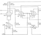
I've taken jcx's approximate AD797 simulation and made a few modifications to it. I blocked all the global feedback by putting a 1e10 Henry inductor in series with the feedback resistor from output to inverting input, and a 1 Farad cap to ground on the non-output side of the inductor. Then I put a loop gain probe inside the "neutralization loop". Here's the schematic and loop gain plot.
Looks like LTP, Schmidt trigger (does not latch due to working points(?), but has a huge output resistance and a voltage gain), Diamond buffer. Negative feedback through C7. C1 forms an integrator with very high output resistance of the Schmidt trigger. It adds stability on highs, but shifts phase of the feedback signal.
Can the amp work at all without a feedback on DC, or sticks to the rail?
Also, a "Diamond Buffer" can't be cured by an external bias to any rail, so I suppose the real thing has a different output stage.
It's too late tonight but I'm on forced time off so you'll have to put up with another one of my explanations soon.😀
In general I wanted just to differentiate from EC which is derived by a small "high" gain amplifier that servos the output stage error to 0, by squirting current through a small series resistor or some such.
Traderbam, that comment was a memory of an old argument at the AES where we got down to a current mirror is "just a three transistor current feedback amplifier".
Wavebourn said:
Also, a "Diamond Buffer" can't be cured by an external bias to any rail, so I suppose the real thing has a different output stage.
Wavebourn have you seen the pictures from my AES preprint? I posted them here (I think) a long time ago. Putting the amp in a CLG of 100 and jamming current into the output made the clearest pictures. A tri-wave rather than sine makes the crossover show up very nicely. Yes, just triple diamond and single folded cascode with gain of 5E6 by "chasing it's own tail". Stuff on IC's matches well enough to count on this.
Scott, it reminds me regenerative receivers Germans used during WW-II when Allies were thinking of them as of obsolete things... They had huge gain and selectivity with much less number of tubes than super-heterodynes had, stability issues were addressed by very accurate layout and proper screening.
No, I did not see that pictures.
No, I did not see that pictures.
Just wind those "ticklers" carefully. 🙂 . I understand what you are saying, but here it's just a super-bootstrapping technique to get very high DC OLG. There is an extra 25pF/50 Ohm pole-zero circuit hidden in there to make behavior at 60MHz or so better, but that is not relevant to the DC/audio performance.
traderbam said:My question to you, Scott, is what choice of Zn, Zc and A make this a FB circuit, if any, and which do not. That is the crux of my challenge to your earlier rejection of the FB label.
Brian
Excellent picture Brian, I see the argument. Drawing A like an amplifier might cause a little confusion. To proceed just think of taking a super diamond stage with infinite current gain and a nonlinear voltage transfer dependent on load and connecting a resistor from input to output. This creates a nonlinear input resistance/current directly related to that nonlinearity. Is this due to feedback or something more like bootstrapping? I might look at your drawing and see a half bridge that nulls the voltage error of the output stage.
So there is a semantic element to this. I didn't double check but I assume your drawing yields that the ouput voltage is gm*Rl independent of A (certainly for .8 < A < 1). That was the point.
As I said I did run this circuit with both current mirror pins brought out. It was a long time ago but I remember with an input gm of 1/100 Ohms or so and 10K resistors instead of compensation caps (just like Dimitri's drawing) I could run the circuit at an open-loop gain of 100. The output stage nonlinearity was nulled even at Rl =100 Ohms. I found the empty box in my stuff last night so the parts are gone.

BTW when we buy your fancy European dishwashers we have to contend with English to metric mismatch. I had one plumber come and cut everything off and then say ef-it you figure it out and leave unpaid.
Interesting how the loop gain plot looks the same as what we've seen for the Miller loops we've been looking at over in the Cordell feedback thread.
Hmm, an inverting transimpedance amplifier with a capacitor from output to input. What could be more Miller-like than that? Of course, there's the added twist that it must act like an integrator with a differential current drive.
Hmm, an inverting transimpedance amplifier with a capacitor from output to input. What could be more Miller-like than that? Of course, there's the added twist that it must act like an integrator with a differential current drive.
It was useful in the past to look at the transfer function of the complete amplifier w/wo Cn (my original drawing). To me "Miller" implies gain, at G~=1 it would seem moot.
scott wurcer said:It was useful in the past to look at the transfer function of the complete amplifier w/wo Cn (my original drawing). To me "Miller" implies gain, at G~=1 it would seem moot.
Scott, I'm talking about transimpedance here. The feedback factor of the minor loop in this case being the transadmittance sCn and the open-loop gain of the minor loop being roughly the transimpedance from pin 8 to the output.
Considered in this way, this is nothing more than a Miller loop enclosing the output stage - similar to, but not identical to, the low-distortion topology of the Smith, Koen and Witulski 1994 article.
for reference here is my earlier simplified ad797 sim analysis and the scope images frome Scott's paper
the sim and my loop gain test is shown in:
http://www.diyaudio.com/forums/showthread.php?postid=1525757#post1525757
my take is that it is useful calling Cn a local positve feedback which effectively cancels the Cc gain roll-off for signals in the mirror/bootstrap/output loop providing a higher "error correcting" negative feedback loop gain around the output stage
and that in general bootstrapping gain enhancement is local positive feedback cancelling an enclosed negative feedback loop and "unmasking" the internal gain of the buffer/follower amplifying device - there is no "free gain" you are limited by the gain of the devices in the loop and you still have to compensate per Bode's criteria
jcx said:My AD797 simplified circuit sim
http://www.diyaudio.com/forums/showthread.php?postid=1525757#post1525757
modified to match the conditions of Scott's AES paper and compared with his pic (from the previous page of that thread)
some scale differences but remarkable congruence of waveform features tempts me to believe the sim can “explain” the bumps at zero (output current) crossing
Av 1000 amp, input to gnd, +/-10 mA triangle ramp pulling on the output (output V =green trace)
top with full 50 pF internal comp limiting high frequency gain
bottom with Scott's “distortion canceling” Cn (increased Vres to see any features)
1st we can dismiss John's characterization of this as crossover distortion, simply run the output stage Class A by changing the output current ramp to +/- 1mA which keeps within the push-pull Class A operating range of the 500 uA output Q bias (to me using the term "crossover distortion" unmodified implies a static nonlinearity)
all John has to do is buffer the output to get this level of linearity, keeping the AD797 in its Class A operating range
again the top trace is without Scott's recommended Cn, lower with Cn
2nd we can see that at 16 Khz Scott's test is pretty fast, so what does the sim show at 100x slower?"
note the V scale is 8 mV full scale, compare to over 100 mVpp error waveform amplitude in the 1 plot without Cn
a little slope change is evident without the Cn cap in the top sim, the bottom looks as linear as could be desired
I think these sims are enough to finger the dynamic charging requirement of full output transistor commutation when running the output devices Class AB as the real “crossover hat” culprit in Scott's AES pics
perhaps external Class A bias would also achive higher high frequency linearity by avoiding the output Q commutation - I would rather use a few more components to make a buffer in the feedback loop after Jung and not have to consider the skewed bias conditions inside the chip and also totally ignore thermal feedback
jcx said:for reference here is my earlier simplified ad797 sim analysis and the scope images frome Scott's paper
the sim and my loop gain test is shown in:
http://www.diyaudio.com/forums/showthread.php?postid=1525757#post1525757
That was a great post. I should have linked to it earlier. Sorry.
Also, just to clarify, the loop gain you plotted was the global loop gain of the entire op-amp and feedback loop. In my earlier loop gain plot that used your simulation, I blocked the global feedback and looked at only the loop gain of the neutralization loop itself.
my take is that it is useful calling Cn a local positve feedback...
I'd argue that it's negative feedback, with the following rationale. With Cn not present, if you source a DC current into pin 8 (the left side of the current mirror), the collector voltage of the right side of the current mirror will go down. Thus the DC transimpedance from pin 8 to the output with no signals applied to the op-amp inputs will be inverting. This is the same as a normal Miller-compensated VAS. The waters are muddied somewhat by the compensation cap, which gives quadrature phase between the sourced pin 8 current and the output voltage even at pretty low frequencies.
- Status
- Not open for further replies.
- Home
- Amplifiers
- Solid State
- John Curl's Blowtorch preamplifier