stinius said:
Total power dissipation @ T=25 deg C =625mW
That's absolute maximum ratings, nor working condition.
Joshua_G said:
That's absolute maximum ratings, nor working condition.
Ummm ... that is all you ever get!
The working power is simply Vds x Id
You then have to work out the temp rise as a function of Tamb and the environment/heatsink.
Joshua_G said:
That's absolute maximum ratings, nor working condition.
Yes that is max rating at ambient T=25C
The rest you will have to figure out, look at something like 5mW /C derate above 25C
The transconductance is essentially 2:1 for n to p. The easy workaround is 2 p-channel devices paralleled for 1 n channel device. It works pretty well. However the input capacitance becomes something like 130 pF, so you need some juice in front of it to get any slew rate.
1audio said:The transconductance is essentially 2:1 for n to p. The easy workaround is 2 p-channel devices paralleled for 1 n channel device. It works pretty well. However the input capacitance becomes something like 130 pF, so you need some juice in front of it to get any slew rate.
2SJ76,7,8,9 has about 120 pF input capacitance, so they are not far off.
We are left with possibly too low power dissipation for an output stage.
In this case, the ZVN4424A and ZVP4424A would be a better matching pair.
They are also available in SOT223 (Suffix G), which is allowed to dissipate 2.5W.
They are also available in SOT223 (Suffix G), which is allowed to dissipate 2.5W.
Those are also interesting and the demonstrate the underlying nature of the devices. The new ones are probably twice the area. They have twice the capacitance, twice the transconductance and 1/2 the on resistance.
How much output bias is necessary? Too much will be counter productive. Enough to drive the lowest resistance and highest capacitance load at the max signal voltage and frequency without and device getting cut off is a pretty near max target. If more is required for linearity then possibly different devices would be a better selection. John's suggestion of peak Beta is a start as is Scott's Ft curve. If peal beta is 1 A and the device won't handle the power (like the mosfets above) look at what happens at appropriate biases.
Also I like to have 10-15 V peak output minimum but any commercial power amp went into clipping at 3V peak or so and more than a few get into real trouble at much higher a signal. Higher output swings may really limit other performance aspects.
Jon Lord said:In this case, the ZVN4424A and ZVP4424A would be a better matching pair.
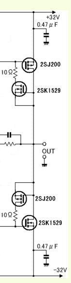
You can't have them both. N/P MOSFETs are either matched for transconductance (typical for "analog" pairs like 2SK1530/2SJ201) and then the have 1 : 2...3 Ciss or charges) or for charges (typical for "switching" pairs like IRF240/IRF9240) and then they have 2...3 : 1 transconductances). The whole trouble is due to the electron/holes mobility ratio which is about 3 and there's no way around this limitation in majority carriers conduction devices like MOSFETs. The same applies to JFETs, look at the Ciss for the 2SK170/2SJ74 pair, having the same 22mS transconductance.
Bipolars do not have the same limitation.
Attachments
Re: Evolve Power Amplifiers
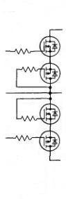
In the first, two of the MOSFETs are always off and the only effect is to add some capacitance to the other MOSFET Crss. The other one seem to level shift with one threshold voltage and add a series capacitance to the equivalent Ciss. They may lead an equal equivalent Crss (or Ciss) for the N and P channel devices (I didn't do a throughout analysis), but to me the price payed (two extra power devices doing essentially nothing signal wise) is way to high. Plus the increased equivalent Crss or Ciss, which is anything but good for the performance.
Just curious, are these snippets from a commercial product? Honestly, the idea seems to be pretty dumb. But then, what do I know 🙂
dimitri said:
What about this:
dimitri said:Or this:
In the first, two of the MOSFETs are always off and the only effect is to add some capacitance to the other MOSFET Crss. The other one seem to level shift with one threshold voltage and add a series capacitance to the equivalent Ciss. They may lead an equal equivalent Crss (or Ciss) for the N and P channel devices (I didn't do a throughout analysis), but to me the price payed (two extra power devices doing essentially nothing signal wise) is way to high. Plus the increased equivalent Crss or Ciss, which is anything but good for the performance.
Just curious, are these snippets from a commercial product? Honestly, the idea seems to be pretty dumb. But then, what do I know 🙂
Bipolars are more similar as complementary pairs but they are still not perfectly identical. The 2n4401 and 2n4403 are very similar but the 2n4401 has a higher ft. Perhaps on an IC they can do better, but probably worse given the tricks necessary. I think its better to design around those limitations than worry about them.
Thats why its hard, I have forgotten most of it. Its like a detailed knowledge of machine language for a Control Data 6600. Not needed much any more. Now that would be a real obscure PHD- a philologist specializing in dead computer languages.
Now, how did I attend to the complementary balance of the jfets over 35 years ago?
And how did Demian address the same problem with mosfets over 30 years ago?
And how did Demian address the same problem with mosfets over 30 years ago?
Also, how did Charles Hansen and I deal with this problem with mosfets in our designs in the 1980's.
And how did Toshiba deal with this problem with its jfets?
And how did Toshiba deal with this problem with its jfets?
Many here, especially my critics, may wonder why I ask these questions about complementary FET matching. It is not to be negative, but to show people who find these questions difficult, that they are significantly behind on how the BLOWTORCH, AYRE, and many other fet topologies actually work, and the problems we have solved over the decades.
I would think that it should be a prerequisite that a certain level of understanding should be attained, before judging what you didn't design, and really don't know much about.
I would think that it should be a prerequisite that a certain level of understanding should be attained, before judging what you didn't design, and really don't know much about.
- Status
- Not open for further replies.
- Home
- Amplifiers
- Solid State
- John Curl's Blowtorch preamplifier