http://documentation.renesas.com/doc/products/transistor/rej03g0903_2sk213ds_a.pdfHi everyone, I hate to say it again, but I was told once, many decades ago, that at least some semiconductor manufacturers used freon baths to test and determine temperature sensitive characteristics of at least some semiconductors. I never saw this in action, but it made sense. A cooled conductive fluid, continuously bathed over a particular device could approximate an 'infinite' heatsink.
Now, what can we do with to TO-92? I need to dissipate 50ma at 30V or 1.5W per unit, to make an effective line stage. Can I do this with device? If not, what is the alternative?
http://documentation.renesas.com/doc/products/transistor/rej03g0122_2sj76ds.pdf
Didn't you use these as an alternitive ?
Last edited:
They won't work very well, because the P channel device does not well match the N channel device in terms of output conductance, AND you get LOTS of second harmonic. You have to cascode to make it work reasonably well.
You see everyone, perhaps a 30 year old design with 'obsolete' parts is not as practical as it first looks. IF I show you the answer, it will beyond most of you to follow or to implement.
Now, what can we do with to TO-92? I need to dissipate 50ma at 30V or 1.5W per unit, to make an effective line stage. Can I do this with device? If not, what is the alternative?
You might have to just break down and parallel two of them.
😎
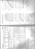
Sorry everybody, I forgot to show the pages of the Supertex device from 1983.
And here they are in proper orientation.
se
Attachments

Also remember that the one lead in particular (usually the drain for DMOS, or the collector for bipolars, or the gate for JFETs) is by far the best heat path to the chip. The ratings are typically for ambient, for which TO-92 is pretty high thermal resistance.You might have to just break down and parallel two of them.
😎
Use of a little copper flag or for the adventuresome, BeO etc. pressed into good contact as close to the encapsulant as possible can provide a remarakble improvement over the ambient rating. Although I am glad that Patrick has done his heatsinks, if you really want to push things I think this is the way to go.
Speaking of paralleling semis, do you find that paralleling devices lower the sonical qualities compared to using only one device (for ex using 4 pcs of 2SK170GR in parallel instead of using one SK170V)?
/S
/S
Two parallel devices AND a freon thermal heatsink! Yes, that should do it! '-)
If you were really serious you could get rid of the plastic. The hardcore CPU overclockers remove Intel's heat spreader to get to the die directly. Obviously not practical.
Heat problems? Now you have a reason to use diamonds: Nano Materials International Corp. : Aluminum Diamond Heat Spreader Demonstrates 25% Reduction in GaN Die Temperature : Article So our high end audio can have gold, silver and diamonds. Real male jewelry.
I support you on that. E.g., why does the copper tube have to be polished?
edit: I see it is on thermal management, the paper, but the question still stands.
Polished for laminar flow designs. There, if not polished, boundary layer thickens.
Therefore the amount of fluid with low velocity close to the tube surface increases.
The heat transfer is hintered.
Even with well polished tube, the flow velocity of thin slice of fluid close to the tube inner walls ends to be small.
They deliberately introduce minute vortex generators for to induce local velocity differentials for to increase the heat transfer rate. (This way of course they add energy to the system, making the effieciency of the whole process lower but this seems not to be their main interest)
George
Three, more practical papers (plain language)
http://www.aavid.com/sites/default/files/technical/papers/Cooling-Key-Chips.pdf
http://www.aavid.com/sites/default/files/technical/papers/how-to-select-heatsink.pdf
http://www.aavid.com/sites/default/files/technical/papers/Bonding-Brazing-Technologies-Electronic-Cooling.pdf
But that would violate your standard that input impedances be 10k or higher.
se
Steve thanks, considered one edge less... you're correct.
Anyway, with low Z of < 100R and a load of > 600R we have enough signal output and enough headroom. Using a TVC we can transform the input impedance from the power amp. Another way would be a gain stage with unity gain - giving up the idea of passive attenuator.
OK well if you stubbornly wont accept the same die in another package, or investigate new technologies; there you go, youve sealed the deal. well done!!
Did you read that JC said "the TO-92 device is about the only one left for sale from Supertex Inc, today."?
I support you on that. E.g., why does the copper tube have to be polished?
The copper tube was a method of getting the ground reference to the front panel while containing all the faraday shielded signal coax cables. The only reason for the continuation of the coax is for crosstalk supression, hence faraday shield. The only reason for the tube is to maintain a circular cross section. If the circular section is distorted, the magnetic field of the tube currents will intrude into the volume of the cylinder.
It is polished to be eye candy, nothing more. No reason to plop an ugly unfinished brass or copper tube here. Polish it to a mirror, then coat it with a laquer to retain the finish. Or, simply use 4/0 steel wool with the tube chucked into a lathe or drill press.
Hi everyone, I hate to say it again, but I was told once, many decades ago, that at least some semiconductor manufacturers used freon baths to test and determine temperature sensitive characteristics of at least some semiconductors. I never saw this in action, but it made sense.
I have seen it in action. Simply because I have done it. Part and parcel of the mil spec game. It was used for isothermal reasons, not to remove heat from the device. Edit: btw, try measuring leakage specs on a device below the dew point in the room. Mil spec temps go significantly below that, condensation below 32 F or zero C kinda mucks up the measurement. Since I had to test chip specifications, even low temp leakage or gain, either from a waffle pack or directly on an unscribed wafer, condensation was a consistent bugaboo. There were nitrogen gas based fridge setups we used as well, but they aren't that easy to work with.
A cooled conductive fluid, continuously bathed over a particular device could approximate an 'infinite' heatsink.
Correction. A particular device attached to an infinite heatsink with a terribly inconsistent turbulent, non linear media.
Well, that's simple.Now, what can we do with to TO-92? I need to dissipate 50ma at 30V or 1.5W per unit, to make an effective line stage. Can I do this with device? If not, what is the alternative?
The power rating of the device is based on junction temperature, the chip mount to a header, the specific chip design in some cases (since the chip is used in another package at higher ratings, we can assume that there is no inherent chip dissipation issue here. For the to-92 device, it is further rated by the length of the leads. It is important to understand how the leads contribute to the theta junction to ambient...ambient being the pad the device is soldered to.
Look at the temperature drop of the leads.
The thermal resistance of a material is:
R = length / (area * K)
some K's (bear with me, this is from 30 year old memories..I have it in a book as well)
K:
Copper:10.2
Alum:5.5
BeO: 5
Alumina : .89
A 1 inch cube of copper:
R = 1 /( 1) * 10.2
R = .098 degrees C per watt.
A 40 mil dia lead 1 inch long: area = .02*.02*pi = .00125 in sq.
R = 1 /( .00125 * 10.2)
R lead = 79 degrees C/watt
So what is the cross section area of the to-92 leads? Is one doing all the work, or are all 3 being used in the calc? And what length do they specify?
jn
Last edited:
Polished for laminar flow designs. There, if not polished, boundary layer thickens.
Therefore the amount of fluid with low velocity close to the tube surface increases.
The heat transfer is hintered.
Highy polished surface is liquid repellent and creates slight turbulences in boundary layer. For optimum laminar flow you would need a surface with "just the right amounf" of granular roughness. "Finely sanded" probably will do.
Can somebody cleave one of the devices open and take a good pic?
I'd like to see if the device is bonded to a continuous leadframe such that the heatflow will be maximum from one lead. What terminal is backside for the chip?
What is the thermal path from the chip to the flat package tab?
Can somebody scope the encapsulation plastic to determine if it is alumina filled?
As a simple first pass, I'd bond the flat directly to sink using Emerson and Cuming 2850 FT and hardener 11 or 9, bend all three leads 90 degrees within 20 mils of the exit point of the package, and make sure the terminal with the backside connection gets much more copper pad surface. For best effort, an aluminum hold down bracket formed to the topside curvature, with screws to the pcboard, use the epoxy to bond the device to the hold-down bracket.
Tis easy enough to build a piece of equipment capable of measuring the die junction temperature with 1.5 watts dissipation at 30 volts, perhaps somebody's interested?
It would certainly help JC out.
jn
Can somebody cleave one of the devices open and take a good pic?
I'd like to see if the device is bonded to a continuous leadframe such that the heatflow will be maximum from one lead. What terminal is backside for the chip?
What is the thermal path from the chip to the flat package tab?
Can somebody scope the encapsulation plastic to determine if it is alumina filled?
As a simple first pass, I'd bond the flat directly to sink using Emerson and Cuming 2850 FT and hardener 11 or 9, bend all three leads 90 degrees within 20 mils of the exit point of the package, and make sure the terminal with the backside connection gets much more copper pad surface. For best effort, an aluminum hold down bracket formed to the topside curvature, with screws to the pcboard, use the epoxy to bond the device to the hold-down bracket.
Tis easy enough to build a piece of equipment capable of measuring the die junction temperature with 1.5 watts dissipation at 30 volts, perhaps somebody's interested?
It would certainly help JC out.
jn
If you're doing a one off you could backgrind down to the lead frame. For our new amp we are using silver filled sintered epoxy on a solid copper slug. There is a new PC board process called "coin" insertion that has a solid copper slug through all layers.
EDIT - "Emerson and Cuming 2850 FT and hardener 11 or 9" Double plus thanks for that, just what I was looking for in a new project. $182 a gallon though, do they have quarts?
Last edited:
If you're doing a one off you could backgrind down to the lead frame. For our new amp we are using silver filled sintered epoxy on a solid copper slug. There is a new PC board process called "coin" insertion that has a solid copper slug through all layers.
Audio amplifier?
- Status
- Not open for further replies.
- Home
- Member Areas
- The Lounge
- John Curl's Blowtorch preamplifier part II