The added 10 ohm resistors were to current limit the driver devices in case the amp was shorted. The original output transistors, in parallel could peak almost 50A, so they could tolerate a momentary short, but the undersized, but fast, driver devices needed to be limited to 2A.
No cap is apparently necessary across the bias stage, for some reason. Maybe, because it works that way as well.
No cap is apparently necessary across the bias stage, for some reason. Maybe, because it works that way as well.
Thanks Mr. Curl 😀
Once I found something strange. I build one particular amp, and when the cap accross the VBE multiplier is plugged out, the amp oscilates. When the cap plugged back in, it stop oscilating. Offcourse this is not for all amps, only for that particular amp 😀
Once I found something strange. I build one particular amp, and when the cap accross the VBE multiplier is plugged out, the amp oscilates. When the cap plugged back in, it stop oscilating. Offcourse this is not for all amps, only for that particular amp 😀
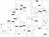
Attached is a schematic for a symmetric folded cascode stage driving complementary MOSFETs directly, as mentioned by JC a few posts earlier. A VGS multiplier was used to set bias. I used the D40D7 ahd D41D7 TO-202 devices for VAS transistors as they are fast and the models were readily available in PSpice. The TO-202 package has 75C junction to ambient thermal resistance, so it can handle a few tens of milliamperes at 20V. I used J113 and J174 for input devices. The input was arranged as non-inverting, but inverting also worked. With the relatively low transconductance of the input stage, no compensation was required. When 2SJ74 and 2SK170 were substituted in the imput stage, compensation caps (22p) were required at the VAS stage to squelch oscillation.
Attachments
This is an interesting design, but it deviates from my course in several ways. First, why cap input? Second, why starve the output fets? Third, why add 100 ohm resistors at the input of the jfets? Fourth, why change the bias track to an unsymmetrical type and adding a 1uF cap across it? Do you know the price and size of 1 uF Teflon caps?  Also, why 200V fets? How about 60V or 100V fets? Why 330 ohms, why not less than 100 ohms?
Also, why 200V fets? How about 60V or 100V fets? Why 330 ohms, why not less than 100 ohms?Mr. Curl, I read somewhere here that Jfets likes quite big resistor on its input (5K? 10K?). Is this noise related consideration (from datasheets)?Third, why add 100 ohm resistors at the input of the jfets?
And, why you choose inverting topology for JC-3?
In J74, K170, K117 datasheet, the biggest specified Rg=10kohm. Near zero in K117 datasheetYou badly interpreted the 2SJ74 datasheet.
A strange one is K30, in the datasheet it has Rg up to 1M, but the lowest one is 100kohm.
Back to practical amp. Borbely design never use such a big Rg. What's the contradiction here?
Jfets do NOT need input resistors. However, this design could use an RFI filter/impedance defining R-C resistor input of 100 ohms and 100pf on the very input.
I chose inverting topology for the JC-3 to LOWER common mode distortion. With cascode devices on the input, this recent design will suffer from common mode distortion. Just another potential compromise.
I chose inverting topology for the JC-3 to LOWER common mode distortion. With cascode devices on the input, this recent design will suffer from common mode distortion. Just another potential compromise.
Should be added that for JC-3 it would be good to reverse speaker wires. Though someone might doubt, it is perfectly audible (listening to -180deg phase inversion).
I think that I misread the current setting. It looks like 1.5A now, rather than .15A that I thought it was set at. That is good!.
Yes, it is 1.5A.
Right now I am testing another output stage, biased at 1.3A. It will work outside global NFB again, one heatsink is 410 x 135 mm, 40 wings.
Right now I am testing another output stage, biased at 1.3A. It will work outside global NFB again, one heatsink is 410 x 135 mm, 40 wings.
Inverting lowered distortion and allowed a PP cap to be used, rather than electrolytic type in feedback loop. The Electrocompaniet was inverting also. It is a minor detail.
It should be said, also, that this design started as a tweeter amp design in a tri amplified system. The tweeter had an efficiency of 108spl/watt. 10W was more than enough, and the input cap could be made very small to limit any low frequency input.
Later, this design was slightly improved and given to Mark Levinson as a small amp design. I was never paid for this design, so I published it many years later.
Later, this design was slightly improved and given to Mark Levinson as a small amp design. I was never paid for this design, so I published it many years later.
One of the nice things about JFET inputs, besides sound quality, is you don't need input coupling caps.john curl said:This is an interesting design, but it deviates from my course in several ways. First, why cap input? Second, why starve the output fets? Third, why add 100 ohm resistors at the input of the jfets? Fourth, why change the bias track to an unsymmetrical type and adding a 1uF cap across it? Do you know the price and size of 1 uF Teflon caps?
Also in John's design the gate leakage currrents cancel each other.
Cheapest Teflon I could find in 1µF is the Solen from Partsconnexion for $64.85:
http://www.partsconnexion.com/catalog/CapacitorsFilm.html
Or one must // two Russian 0.47µF , but they are HUGE!
There will be no problem to get 2 x 30W/8 ohm and 2 x 60W/4 ohm from the schematic posted here. And 21193/94 whitstand 30A peak. I believe it could serve well as home amplifier, and it should beat the A-30 !! 🙂D 😀 😀)
Hi Wrenchone,
I do not think Q3 (or Q4) could be considered as a folded cascode.
It is a standard voltage driven common emitter by the potential difference across the voltage across R2 and R3 (or R4 and R5), its base is not at a fixed potential referenced to power supply voltage, ground neither J1 and J2 (J3 and J4) sources node.
QSerraTico_Tico said:
... you don't need input coupling caps.
You do. There is no servo, and the circuit is simple. Without cap, you will multiple offsets by system CL gain, which is no good.
- Home
- Amplifiers
- Solid State
- John Curl amp