I also have this J.L.H. Mosfet Amp DIYed in the mid 80s. Since Duran Duran were making hits.😀
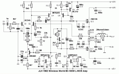
Its in great condition and has very good parts quality. I have found the schematic on the Web and noted the values on it. See it attached. *Q13 is drawn upside down, drain should go to -V.
After I have given it a look inside, I saw that C1 is bypassed (but there is a DC sensing plus time delay, working relay circuit at the output), R1 is 47k, R2 is 1k8, R18 is 27k, there is no L1,R10. Also there is only +/-60V both for drivers and output but with split bridges and filter caps from a common 300VA toroidal secondary. So it must be giving less power than spec.
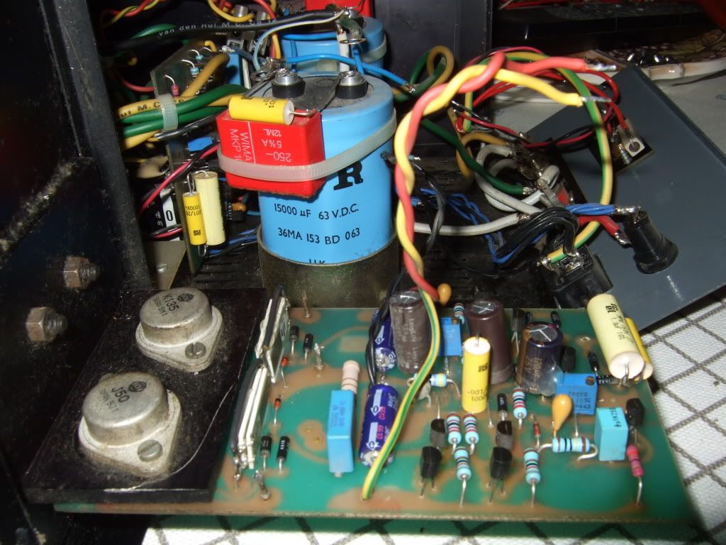
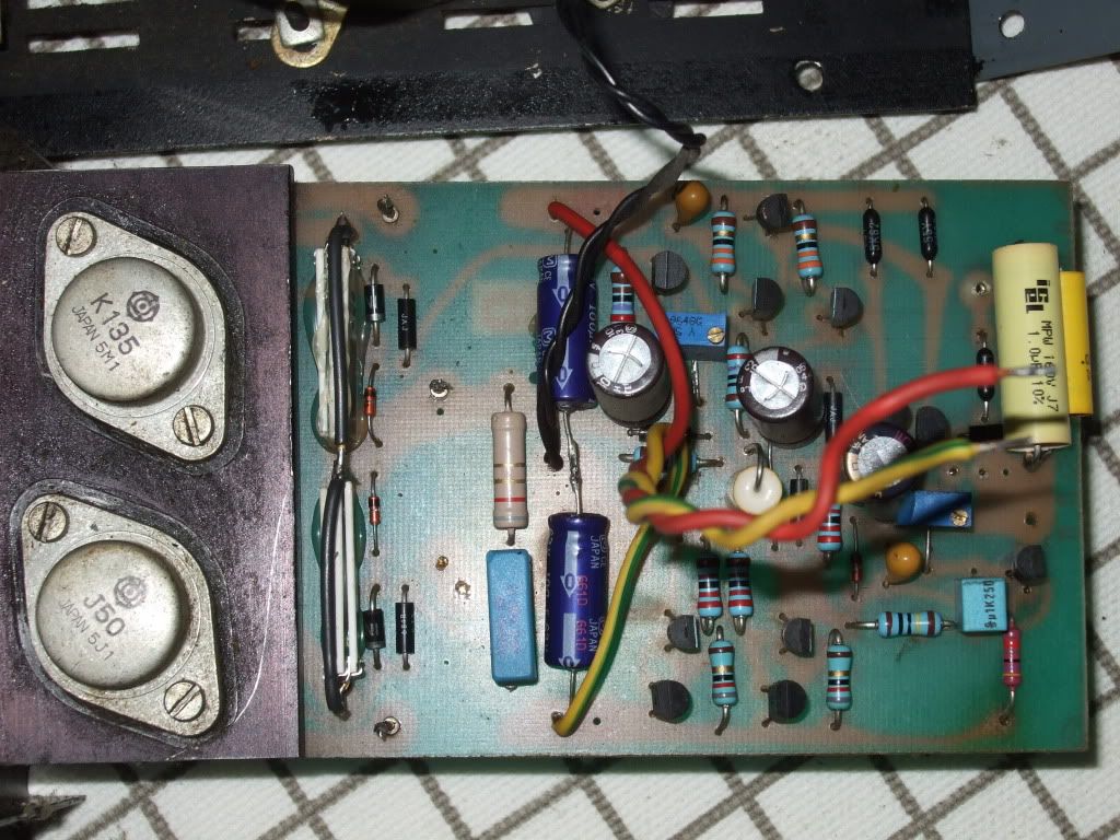
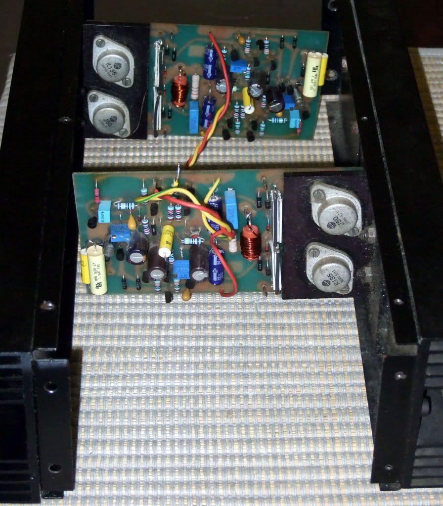
Bad thing is that is giving 0.2% THD at 1W on 8R. I have found that Q1,Q2 are not 65V Vco BC546Bs on the actual boards but probably due to some mistake, 45V Vco BC550Cs. Those are not supposed to hold the DC (just 0.7V drop across the 5k6 loads) but the amp works. The grounding and noise are excellent. No hum bands and -130dB noise floor relative to 1V RMS 0dB. The offset is negligible on both channels and there is proper 100mA bias through the venerable power Hitachis.
My questions are:
1. Can the high THD be a function of the improper(?) BC550s? I will get some BC546s soon and disassemble the amp. Can there be any other reason to look for, if the THD does not improve?
2. Are there any expert suggestions on changing something for the better? The PCBs are nice green epoxy, maybe not changing the schematic but manipulating some values or doing some small scale easy changes?
Thanks in advance.
Its in great condition and has very good parts quality. I have found the schematic on the Web and noted the values on it. See it attached. *Q13 is drawn upside down, drain should go to -V.
After I have given it a look inside, I saw that C1 is bypassed (but there is a DC sensing plus time delay, working relay circuit at the output), R1 is 47k, R2 is 1k8, R18 is 27k, there is no L1,R10. Also there is only +/-60V both for drivers and output but with split bridges and filter caps from a common 300VA toroidal secondary. So it must be giving less power than spec.
Bad thing is that is giving 0.2% THD at 1W on 8R. I have found that Q1,Q2 are not 65V Vco BC546Bs on the actual boards but probably due to some mistake, 45V Vco BC550Cs. Those are not supposed to hold the DC (just 0.7V drop across the 5k6 loads) but the amp works. The grounding and noise are excellent. No hum bands and -130dB noise floor relative to 1V RMS 0dB. The offset is negligible on both channels and there is proper 100mA bias through the venerable power Hitachis.
My questions are:
1. Can the high THD be a function of the improper(?) BC550s? I will get some BC546s soon and disassemble the amp. Can there be any other reason to look for, if the THD does not improve?
2. Are there any expert suggestions on changing something for the better? The PCBs are nice green epoxy, maybe not changing the schematic but manipulating some values or doing some small scale easy changes?
Thanks in advance.
Attachments
Definitely replace teh bc550's! I'd probably upgrade the MPSA43/MPSA93's to the MPSAW42/92's as they have a 1W package that dissipate a bit more heat.
I'd definitely replace the electrolytic capacitors as well... the PSU ones might really need it.
I'd definitely replace the electrolytic capacitors as well... the PSU ones might really need it.
Will do. I wonder how it works with over max Vco NPNs though... maybe due to the very low current. I run a sim for the first and second stage including the feedback to the tail Njfet CCs gate and it actually confirmed the low voltage drops. They may very well be pushed I guess. Do you have any experience with this John Linsley Hood design and its proper performance?
Here I found the original if it rings a bell to UK guys mainly
Here I found the original if it rings a bell to UK guys mainly
that schematic says V mosfet.
But the output devices that JLH specified are Lateral devices.
JLH published a number of variations of this Lateral FET amplifier.
The later ones were called 80W amplifiers.
JLH was a brilliant designer.
I hold him in high esteem.
Search under his name John Linsley Hood and you will find many of his designs of this Forum.
Q6 needs to be changed to a PNP type and oriented to place the VR on the BE side of the multiplier.
This early circuit could be updated to the very similar 80W version which is still made with minor modifications by Williams Audio?
I doubt you will want to copy the 4u7//4u7F and the very high resistor values used in the NFB leg.
Note the lack of Cdom (Miller comp cap), a very British way of designing amplifiers.
Hello Andrew. Thanks.
Is the high THD indeed coming from the false use of BC550s in the particular build?
You mean the one with the 150k Rf so to use polyprop 10uF for the DC/AC cap in the feedback as it was suggested to JLH by Bobken?
The current one has feedback there though (22k) and I think it helps the situation.
Is the high THD indeed coming from the false use of BC550s in the particular build?
You mean the one with the 150k Rf so to use polyprop 10uF for the DC/AC cap in the feedback as it was suggested to JLH by Bobken?
The current one has feedback there though (22k) and I think it helps the situation.
Hi AndrewT
---JLH published a number of variations of this Lateral FET amplifier.---
This one is quite different from the other JLH Mosfet Designs published later and which had a Mos VAS.
Here there is positive feedback around the NFB loop. To me, the most intriguing design of his author.
I built it around the date of publication. I can't say much about the sound, but when first trying it I was very surprised by its extremly low DC offset, less than 1 mV. I have to state that I matched the pairs and did not use the 470 Ohm DC balancing pot at the LTP.
I can see many similarities between this and JLH's other versions.forr said:Hi AndrewT
---JLH published a number of variations of this Lateral FET amplifier.---
This one is quite different from the other JLH Mosfet Designs published later and which had a Mos VAS.
So much so that if it had not been identified as a JLH many who know his work would guess it as one of his designs.
I just got 4XBC546Bs with hfe between 260-330. But I also pulled out old Philips ones with hfe between 80-110. What would be best to try? I guess that the old design was tested with lowish hfe 447s of that era.
I guess they would push the Vas stage if high hfe? Maybe that is the reason of high THD with the BC550s, because of a marginal stability issue due to excessive closed loop gain, translated to more than intended feedback?
P.S. I am changing the title and schematic to L-Mosfet.
P.S. I am changing the title and schematic to L-Mosfet.
the voltage drive into the VAS is determined by the current output from the LTP and the resistor value of the collector load.
Judging by the 5k6 collector loads the collector currents must be very low. Probably ~ 150uA. Tail current ~ 300uA.
That 470r balancing VR in the tail gives an effective 235r for the LTP emitter resistors. That combined with the low Ic will give a fairly low first stage gain.
Judging by the 5k6 collector loads the collector currents must be very low. Probably ~ 150uA. Tail current ~ 300uA.
That 470r balancing VR in the tail gives an effective 235r for the LTP emitter resistors. That combined with the low Ic will give a fairly low first stage gain.
Ok, I will change the non specified 550s to high hfe 546s, will restore the proper values of some resistors, will restore the output series Zobel, will renew some electrolytics. Will trim it again, measure it in an FFT loop and see if THD has gone down. Anything else suggested before I take it apart?
Output resistor
Hi Salas,
The schematics you use does not have the 0.22 ohms output resistor as does the original JLH design. This resistor sure has an impact on the sound since it reduces a lot the damping factor.... anyone would like to comment here?
Hi Salas,
The schematics you use does not have the 0.22 ohms output resistor as does the original JLH design. This resistor sure has an impact on the sound since it reduces a lot the damping factor.... anyone would like to comment here?
There is no provision for it on my pcb too, so I will leave it out. JLH never did something without a reason though. Maybe it was damping back EMF better.
This is the JLH Mosfet amp many times published with almost no variation
http://www.tcaas.btinternet.co.uk/EWWW6-93.gif
It is very different from the one discussed here, details of which were publiseh in June, July and August 1982 issues of Wireless World.
The JLH thinking started from a double diff stage with current mirror loading the second stage, à la Hitachi.
But JLH was worried by the lack of a well defined quiescent current in the Vas stage and prefered a CCS loading.
So he went to this very curious double VAS, one supplying the output stage as usual, the second one providing positive feedback around the NFB.
Quoting what he wrote :
"While it is difficult to envisage any standard constant-current source which would have the same dynamic advantage as a current mirror active load, ananalysis of the behaviour of such an active load (which is that of positive feedforward from the parallel antiphase limb) in an amplifier having an overall negative-feedback loop, shows that it is substantially identical in its characteristics to any arrangement giving similar gain increase by 'positive feedback within the negative-feedback loop'. This is a circuit technique of some antiquity and more widely used, deliberately or inadvertently, than one might guess."
Good Build
In very nice shape indeed. Icel, 1000V film & foils, high ripple LCRs, PP snubbers, non inductive Rsource, Panasonics, Elnas, Vishay low ppms (black ones), Supra, VDH, Kimber. The parts quality has been upgraded in the 90s. Gotta make this amp measure properly. It may play very nice music.
Will substitute the front end and measure it again for THD as first step of action. Will keep you posted.
Ok, it got the BC546Bs in, Motorola 2N5461 CCS (there was an NTE326 there, drain up, they are supposed to be symmetrical but I put the new ones source up anyway), Polysterene 1n on input RC filter, 10R//2uH measured & matched series Zobels. Lets see how it tests. Have to put the PSU back together first and balance offsets. Probably tomorrow.
- Status
- Not open for further replies.
- Home
- Amplifiers
- Solid State
- JLH 100W L-MOS 2nd Life