Hey.
I have read so much good words about JLH 10 Watt,
so I want to build one, but I think there is plenty of versions
of this amp.
So to get things a little easyer:
Is this the "best" and most updated version (fig. 2):
http://www.tcaas.btinternet.co.uk/jlhupdate.htm
If not, where can I find it?
I have read so much good words about JLH 10 Watt,
so I want to build one, but I think there is plenty of versions
of this amp.
So to get things a little easyer:
Is this the "best" and most updated version (fig. 2):
http://www.tcaas.btinternet.co.uk/jlhupdate.htm
If not, where can I find it?
Hi Rodger-K
I built that version with two pairs of 15003, four transistors and
used the capacitance multiplier supply from Rod Elliot.
It came out really wonderful, the only thing is you have to use a heafty
heatsink because the idle current is about 3 amps and you need to dissipate all that heat. Used two transformers, one per chanel
and the supplies are fully regulated as per Rod's circuitry.
Very high quality amplifier which drives my electrosctatic speakers
only on the winter time, it doesn't like the high summer temperatures.
Good luck, it's a well worth project to acomplish.
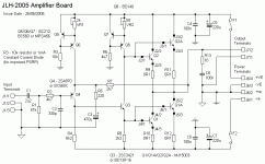
JLH Schematic
Here is the schematic of the JLH amp I built. Well, I'm still building it. But I have spent quite a few hours listening to it. It sounds very good.
I have PCB Gerber files as well. Geoff Moss sent me these a while back, but tells me that there are no newer versions available, at least at the moment. I had the boards built by Olimex.
Attachments

JLH Bias adjustment procedure
...and here's the procedure Geoff advised me when I was bringing up the amp. I started with very low voltage and a current-limited power supply, then switched to my big supply for the final adjustment.
If you are building the high power version with parallel output transistors, with VR2 set to maximum (50R), I would expect each output transistor to be passing about 300mA (ie there will be about 30mV across each of the 0R1 resistors) when the supply rails are at +/-10V. This does not vary very much when the rails are +/-22V. The actual current depends on the gain of the individual output transistors. The Q7/Q8 ccs will supply a current to the bases of the output transistors which is equal to the Vbe of Q7 (~0.6V) divided by the value of VR2, so with VR2 at 50R the ccs current will be ~12mA. This gives 3mA into the base of each output transistor and if it's gain is 100 (a typical value) the collector current will be ~300mA.
As for initial setting-up, before power is first applied I would adjust both VR1 and VR2 for maximum resistance. After power is applied, VR1 is adjusted to set the output dc offset to near zero and the quiescent current (and
current sharing) checked by measuring the voltages across the 0R1 resistors. If all seems well, VR2 is adjusted to raise the quiescent current to, say, 1A. After a short period to allow the transistors to warm up, the output dc
offset is reset to near zero by adjusting VR1. Back to VR2 again and raise the quiescent current to, say, 2A. Wait a while and reset the output offset.
Unfortunately, the adjustments of VR1 and VR2 interact and so the setting of the quiescent current and output dc offset is an iterative process but after about four steps you should be able to get the current and offset somewhere
near to the required values. At this point, it is necessary to let the amp idle for an hour or so in order to ensure that thermal equilibrium has been reached and that the amp is at its normal operating temperature. The
quiescent current and output dc offset are now trimmed to the required values. These are best rechecked after a further settling period (say about 30 minutes).
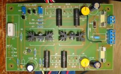
Geoff PCB
I just wanted to add that I have built my JLH using Geoff's PCB and it works. There are no errors and you can use it with confidence. Mine is 15W version.
I just might add that the PCB of Geoff is designed for a monoblocks and you could (like me) find a little bit difficult to mount everything in if your transistors are on one side for one channel and on the other side for the other...
Pred
They are the same version. You need two sets of output transistors for higher power. The layout is what I posted earlier. If you want Gerber files email me. I don't have a parts list, you'll have to make one from the schematic (there are some options).roger-k said:Is there a place where I can download the PCB-layout and partlist for the 15W version?
Hi Pred!
Which PCB do you speak???
Is it public??
Greets:
Tyimo
I just wanted to add that I have built my JLH using Geoff's PCB and it works.
Which PCB do you speak???
Is it public??
Greets:
Tyimo
I suppose paulb will send you the schematics and layout. If not, I would have to ask Geoff for permition it is his design.
About the options you can see from the layout. You can use different transistor Q4 and there are two provisions for different pinout. Almoust all capacitors have two or three holes so you can use different sizes. R3 is either a resistor or current source diode.
Pred
About the options you can see from the layout. You can use different transistor Q4 and there are two provisions for different pinout. Almoust all capacitors have two or three holes so you can use different sizes. R3 is either a resistor or current source diode.
Pred
Geoff has given me permission to send copies of the PCB layout Gerber files to anyone interested. This corresponds to the schematic and layout I posted a few days ago. I am fairly sure this is the same PCB used by Pred.
Roger, I just sent you a copy. Please let me know if it is what you are expecting. Others feel free to email me.
Geoff is not in a position to contribute more of his time, as much as he would like to, as his health has not been good lately. I do know he keeps any eye on the forum and so I would like to say a heartfelt thank-you to Geoff for all the work he has done in making this design and his entire website available to us DIYers.
Pred!
O.K. now I understand that you are speaking about the 2005's circuit. For me the 15W version means the original one from 1969.
I am interested to that one.
Greets:
Tyimo
I just wanted to add that I have built my JLH using Geoff's PCB and it works. There are no errors and you can use it with confidence. Mine is 15W version.
O.K. now I understand that you are speaking about the 2005's circuit. For me the 15W version means the original one from 1969.
I am interested to that one.
Greets:
Tyimo
A question about heatsink for Q3 and Q8
Hi.
Can I have Q8 and (3 at tjhe same hestsink as the main-transistors? (in the low-power version).
Or is this unfavourable?
Hi.
Can I have Q8 and (3 at tjhe same hestsink as the main-transistors? (in the low-power version).
Or is this unfavourable?
roger-k said:I mean: Can I have Q3 and Q8 at the same heatsink as the main transistors?
I think you can but the layout will most likely compromised.
There could be more dc-offset variation between cold/hot as a result, possibly more variation in Iq too but I am guessing here.
As Iq variation between cold/hot is influenced by transistor temperature rise and as dc-offset is in turn influenced by Iq it might be best to play safe unless the main heatsinks are massive or Iq is kept low. I use small clip-on heatsinks for Q3/8 which keeps their temperature rise (and I assume resultant dc-offset variations) lower than I imagine would be the case had they been mounted on the main heatsink.
Tim.
Ok. Tanks.
That sounds sensible, so I will use two small heatsinks for Q3 and Q8.
I have one more question:
http://www.tcaas.btinternet.co.uk/jlhupdate.htm
Down on this page there is a table which show the relations between voltage and output power.
Is this table only for the high power version or is the relations the same for the 10 or 15 watt version?
If not, what voltage do I need to get 10W and 15w?
- Home
- Amplifiers
- Solid State
- JLH 10 Watt class A amplifier