tschrama said:Hi Geoff,
How do you feel about a MOSFET version? Are you allreaddy convinced yet that it can work, be it in a diffrent manner?
Thijs
It seems I am somewhat behind with replies in this thread, sorry about that.
I have no doubt that a MOSFET version can be made to work, and your schematic seems to work well from the limited simulations I have done so far.
When I first tried simulating a MOSFET output stage a year or two back I found the circuit to be rather 'twitchy', that is to say relatively small variations in component values caused a fairly large change in bias currents and voltages.
Also, as you have found in practice, additional compensation was needed in order to obtain suitable stability margins. This meant that the open-loop bandwidth was reduced so that it became similar to many other designs. The standard JLH has an open-loop bandwidth in excess of 20kHz and I believe this is one of the reasons for its superior sonic performance.
Having found these two shortcomings, I didn't pursue the MOSFET option any further, though I'm glad to hear that you and Millwood have achieved some success with this.
Geoff
quote:
Originally posted by Geoff
You refer to distortion and the fact (sorry, your assertion) that it is not affected by the use of unmatched output transistors. Have you actually read Table 2 of the original 1969 article which gives the results of THD measurements for matched and unmatched output devices?
millwood said:
Yes, I have. all I am saying in this "academic" exercise is that 1) gain matching isn't required for this to work; 2) in theory, this circuitry does not require gain matching; 3) it does not require the current matching that x-pro and you had indicated.
You again seem to be basing your opinion on a MOSFET output stage as opposed to the original circuit. Gain matching of the output BJTs in the proper JLH circuits is required to:
1) Minimise distortion
2) Maximise efficiency by providing the widest range of push-pull working.
As I demonstrated previously, excessive mis-match between the output BJTs can lead to a peak output current that is no greater than (or even less than) the quiescent current. The whole point of a push-pull circuit is that efficiency is improved by enabling the peak output current to exceed the quiescent current. If this benefit is lost, you might as well build a single-ended design.
if you are interested in a constructive discussion, I would love to hear your view. Otherwise, I suggest that you leave your attitude at home.
There is no attitude other than a desire to prevent erroneous information from being presented as fact, or to correct it if already posted, so that other (possibly less experienced) readers will not be misled.
Geoff

millwood said:
there is no magic in the 1.3-1.6 figure.
a class a should swing the full output in its linear range. Take my amp for example. It has a gain of 10x, the same with the original jlh design.
Nobody said there was any magic. I merely pointed out that, whereas a perfect push-pull Class-A output stage would deliver a peak output current of twice the quiescent current, the JLH circuit is more limited in its capabilities.
The original JLH, and the 1996 update, have a gain of 13.3 not 10 (feedback resistors 2k7 and 220R).
so a 1vp signal will generate 10vp on the output, or a 20vp swing. On an 8-ohm nominal load, that's 20/8=2.5amp. Assuming that the linear range for the transistors start at 0, the Iq should be set at the middle of the output range, or 1.25amp.
However, very rarely a transistor starts out to be linear to you may want to overbias a little. that means the bias should be slightly over 1.25amp. My listening test shows that bias between 1.2 - 1.5amp tends to be optimal, or 1x - 1.3x of peak current output (10v/8ohm).
if we are using perfect transistors, the ratio should be exactly 1x.
I don't think you really mean that the optimal bias is 1x - 1.3x of peak current for this circuit. That would be applicable for a single-ended output stage (though even then 1.3x might be a bit excessive).
With perfect transistors in a perfect push-pull circuit the ratio should be exactly 0.5x not 1x (assuming you are still referring to peak output current).
Geoff said:There is no attitude other than a desire to prevent erroneous information from being presented as fact, or to correct it if already posted, so that other (possibly less experienced) readers will not be misled.
Geoff
let's me summarize some "assertions" that have been made so far:
1) the mosfet is a push-pull by millwood / tschma: I haven't heard any convincing argument why it is not.
2) the mosfet works by millwood / tschma: duh!
3) the original jlh is symmetric by x-pro: not the least bit. for the driver, it is a common collector for the upper device and common emitter for the lower device. For the output, it is just the opposite.
4) current matching in the jlh1969 by x-pro/tschma: a) the jlh doesn't require that to work; b) unless you disregard bias settings and select the resistors carefully, you will not get the current to match perfect. c) even if you do, there is no assurance that current match will be maintained throughout various work range as the upper and lower load for the driver aren't perfect current sources.
5) the lower mosfet is a current source by x-pro: not the least bit. It pulls just as hard as the upper one pushes, as evidenced by both empirtical and simulation data.
6) the mosfet is thermally not very stable by x-pro: if it is, I haven't seen it in real life.
7) the mosfet is quite sensitive to power supply ripple by x-pro: if it is, I haven't seen it in real life.
8) gain matching required for the jlh to work to achieve "optimum performance" by geoff: yes and no. In the context of our particular discussion where "gain" is degenerated into one constant over the operating range, gain-mismatching is not required to minimize distortion. Graham later presented an argument on "characteristics" and I agree with him that you will likely gain with "characteristics matched" output transistors.
9) the bootstrap cannot be removed by geoff: I trust that you have seen fig 2 in the original jlh article. You will have to take your argument up with him on that, 🙂. And yes, I took out that bootstrap resistor in my amp. it worked, with heavier load on the lower output device.
10) the phase splitting ceases if mosfets used as output by geoff: duh!
11) push-pull ceases if mosfets used as output by geoff: duh!
12) jlh1969 unable to go into class ab when overdriven by tschrama and graham: it appers to be partially true - it is unable to go into class ab on the negative half but will do so on the positive half.
13) for the jlh to work, phase splitting may not be perfect (I don't recall who said this): phase splitting is probably the single most important point of this design. If it doesn't hold, the push-pull goes away.
If you think I made claims that aren't true in your view, I would like you to list them out and tell me why. By doing this, we all gain a clear understanding of how the circuitry works and prevent misunderstanding by anyone.
Merry chrismtas to anyone.
millwood said:
BTW, does the push-pull analysis in your reference use all npn or all pnp devices?
Graham referred you to, as he put it, a "70-odd year old edition of ......". I don't think that npn or pnp is exactly relevant, do you?
First of all, the bias for the output stage in the JLH1969 is NOT constant. Had JLH used two perfect current sources as the collector and emitter load for the driver, or one perfect curent source as the collector load and eliminate the emitter resistor for the driver, as Geoff had suggested, I would agree with you. The matter of fact, unfortunately, is that he used two resistors (well, one bootstrap network + one resistor) in his design.
The bias for the output stage in the JLH 1969 *is* substantially constant due to the provision of the bootstrap arrangement. Except at the frequency extremes when the impedance of the bootstrap capacitor becomes significant, the voltage across the bootstrap resistor is constant (within the limits of the variation in Vbe with Ic for Tr2). If the voltage across this resistor is constant, the current through it must also be constant.
Again, going back to the assertion that the MOSFET version isn't a push-pull, I am of the view that it is completely wrong. I am also of the view that the orginal jlh design is better suited for voltage driven output devices like mosfets.
I don't think anyone has said that a MOSFET version, when correctly implemented, doesn't operate in push-pull. What it doesn't do is work in the same fashion as the original JLH design which uses an accurate current phase splitter to drive the output BJTs directly.
Geoff said:With perfect transistors in a perfect push-pull circuit the ratio should be exactly 0.5x not 1x (assuming you are still referring to peak output current).
we are talking abou the same thing in two different world. In a push-pull with two rails, the maximum current on the load is the Iq when one of the output devices starts to shut off. so the current on the load swings from -Iq to +Iq.
You are thinking about the single rail world where the current on the load swings from 0 to +Iq, with the 1/2 Iq as the mid point.
We arrived at the same conclusion essentially.
Geoff said:I don't think anyone has said that a MOSFET version, when correctly implemented, doesn't operate in push-pull.
thanks for the clarification. I for one don't know of one thing that works but is implemented correctly. so that might just be some definitional things, 🙂.
I am happy to see that 1) we have concrete evidence, both emirically and in reality, that the mosfet version of the jlh1969 circuit works; 2) the mosfet version seems to be gaining acceptance in the jlh community, if the above statement of yours is of any indication.
and as I had stated earlier, a voltage driven device like the mosfet may be a preferred output device because of the Zout assymetry inherient in the jlh design.
thermal stability
I have ran my mosfet jlh1969 for about 48 hours by now, under various conditions. I take frequent voltage readings off the source resistors of the mosfets, usually a couple of hours during the day and none at night.
I got 0.24 - 0.25v readings when this thing idles in my unheated garage, next to an open window (outside temperature is about 30-40F). when idled indoor (about 65-70F), it read about 0.24 - 0.26v, and at one time it got to 0.27v.
I now feel much better to leave this thing on all the time.
sorry, I meant to see incorrectly. My bad.millwood said:thanks for the clarification. I for one don't know of one thing that works but is implemented correctly.
millwood said:I thought about this class ab thing a little bit more.
let's make an assumption: the Iq on the driver stage is significant larger than the base current for the two drivers: in my mosfet version, the iq for the driver is 40ma.
Yet again you seem to be confusing your MOSFET version with the original design. With the BJT output stage, you cannot increase the quiescent current of the drive stage so that it is significantly larger than the base current for the two output transistors (I assume your reference to two drivers was a typo), without reducing the value of driver transistors emitter resistor to a very small value (around 15ohm if you want the driver current to be twice the total base current).
This is likely to seriously degrade the distortion and will certainly significantly restrict the negative voltage swing available into low (4ohm) impedance loads.
In short, the orginal jlh can swing into class ab on the positive side but not able to do so on the negtive side. I believe the mosfet version faces the same limitation (more so I think because the mosfet version isn't as efficient).
This isn't Class-AB working, it is asymmetrical clipping.
millwood said:
we are talking abou the same thing in two different world. In a push-pull with two rails, the maximum current on the load is the Iq when one of the output devices starts to shut off. so the current on the load swings from -Iq to +Iq.
You are thinking about the single rail world where the current on the load swings from 0 to +Iq, with the 1/2 Iq as the mid point.
We arrived at the same conclusion essentially.
Rubbish.
Iq (quiescent current), by definition, is the current passing through the output transistors at idle, ie when no signal is present, so how can one of the output be about to switch off.
It doesn't matter whether the amplifier has a single rail or dual supplies, the quiescent current is the same. For a single-ended amplifier, the peak output current is equal to the quiescent current. For a (perfect) push-pull amplifier the peak output current is equal to twice the quiescent current.
millwood said:
let's me summarize some "assertions" that have been made so far:
1) the mosfet is a push-pull by millwood / tschma: I haven't heard any convincing argument why it is not.
As I said in a previous post "when correctly implemented". If, for example, the driver emitter resistor is not correctly sized the circuit will still work but you will not get push-pull action.
5) the lower mosfet is a current source by x-pro: not the least bit. It pulls just as hard as the upper one pushes, as evidenced by both empirtical and simulation data.
Only if the circuit is redesigned so that it is correctly implemented.
8) gain matching required for the jlh to work to achieve "optimum performance" by geoff: yes and no. In the context of our particular discussion where "gain" is degenerated into one constant over the operating range, gain-mismatching is not required to minimize distortion. Graham later presented an argument on "characteristics" and I agree with him that you will likely gain with "characteristics matched" output transistors.
I have covered this in a previous post. Gain matching of the output BJTs is necessary to ensure minimum distortion and maximum range of push-pull working (efficiency, the reason why a push-pull circuit is used in the first place).
9) the bootstrap cannot be removed by geoff: I trust that you have seen fig 2 in the original jlh article. You will have to take your argument up with him on that, 🙂. And yes, I took out that bootstrap resistor in my amp. it worked, with heavier load on the lower output device.
Fig 2 in the original article was a conceptual diagram showing (with Fig 1) the progression from a single-ended output stage using a resistor for the collector load, through a choke then active load and finally to a push-pull arrangement. Fig 2 was never intended as a working design. However, the driver collector resistor could be considered as an approximation of a constant current source if the supply rail voltage were made high enough. However, the positive voltage output swing would be unnecessarily restricted.
The bootstrap capacitor must remain in the original JLH version if the amplifier is to perform as intended for two reasons.
1 As explained in a previous post, it provides the (nearly) constant current required for the current phase splittter to work.
2 It enables a higher positive voltage output swing thus improving the efficiency of the amplifier.
10) the phase splitting ceases if mosfets used as output by geoff: duh!
Please quote me in context. I said the current phase splitting would cease when MOSFETs are used unless suitable resistors are connected between the gate and the source to convert the current from the phase splitter into a voltage to drive the MOSFETs.
11) push-pull ceases if mosfets used as output by geoff: duh!
Again I am quoted out of context. I said the push-pull action generated by a current phase splitter ceased, which it does.
12) jlh1969 unable to go into class ab when overdriven by tschrama and graham: it appers to be partially true - it is unable to go into class ab on the negative half but will do so on the positive half.
The inability to go into Class-AB (for a BJT output stage) is not *partially* true. We are dealing with signals which are both positive and negative and so both directions must be able to work in this fashion if the output is to be Class-AB. As I said before, what you are describing is asymmetric clipping.
If you think I made claims that aren't true in your view, I would like you to list them out and tell me why. By doing this, we all gain a clear understanding of how the circuitry works and prevent misunderstanding by anyone.
You have made many claims that are either untrue or misleading. I think I, and others, have already pointed out most of these, sometimes on several occasions, but you appear to disregard anything that doesn't fit in with your prreconceived ideas about this circuit.
You have never built the original BJT design and are constantly confusing the issue by inferring, or catagorically stating, that your comments regarding the MOSFET version are equally applicable to the original 1969 version when clearly they are not. The MOSFET output stage does not operate in the same manner as the original BJT one unless the I/V resistors, mentioned above and previously, are added and then the circuit operation becomes similar, ie the driver is working as an accurate current phase splitter.
some preliminary simulation results on replacing the BJT driver with a MOSFET in the mosfet JLH1969:
1) THD at 0.09% with the BJT driver (MJE15030);
2) THD at 0.11% with IRF510 as the driver;
3) THD at 0.94% with IRF540 as the driver.
Both IRF510/540 will work as a drop-in replacement for the MJE. No changes to the rest of the circuitry.
It appears that a small to medium power mosfet with small input capacitance is the way to go for the driver.
The only problem with the IRF510 is that is a little bump at 2mhz with the 510. Needs more investigation.
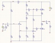
Complementory MOSFET JLH1969
here it is, on paper anyway.
some performance number per my simulation:
THD: 0.12% @ 1Khz, 0.14% at 5khz, 0.21@ 10khz, 0.39% 20khz.
frequency response dead flat to 700khz, and goes to -3db at 1mhz+.
the Iq is set at 750ma, a little bit on the low side. so there is room for improvement, 🙂.
here it is, on paper anyway.
some performance number per my simulation:
THD: 0.12% @ 1Khz, 0.14% at 5khz, 0.21@ 10khz, 0.39% 20khz.
frequency response dead flat to 700khz, and goes to -3db at 1mhz+.
the Iq is set at 750ma, a little bit on the low side. so there is room for improvement, 🙂.
Attachments
millwood said:some preliminary simulation results on replacing the BJT driver with a MOSFET in the mosfet JLH1969:
1) THD at 0.09% with the BJT driver (MJE15030);
2) THD at 0.11% with IRF510 as the driver;
3) THD at 0.94% with IRF540 as the driver.
Both IRF510/540 will work as a drop-in replacement for the MJE. No changes to the rest of the circuitry.
It appears that a small to medium power mosfet with small input capacitance is the way to go for the driver.
The only problem with the IRF510 is that is a little bump at 2mhz with the 510. Needs more investigation.
You do not mention the frequency/power for your simulated THD figures, but the increase when changing from a BJT to a MOSFET is similar to that which I have obtained in simulation.
JLH used a MOSFET as the VAS transistor in one of his later designs (VN1210M) and I believe Zetex make some good small-signal MOSFETs. If I remember correctly, Fred (or it may have been Jocko) recommended a (some?) particular Zetex device some time ago in another thread.
We really should have something better to do on Christmas Day afternoon/evening than spending the time posting here 🙂
Re: Complementory MOSFET JLH1969
I'm not sure that it is appropriate to call this "Complementory MOSFET JLH1969" since your circuit is more akin to some of JLH's later designs, albeit with the output stage biased into Class-AB (though with a fairly high Class-A bias component in at least one case).
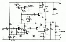
Jlh produced several designs based on the Class-A input stage ranging from the 15-20W published in 1970 to a 270W that saw the light of day in 1975.
A 30W design was published in HFN in January 1980 which was subsequently updated the following December to use MOSFETs in the output stage. I have attached the schematic for this.
You will see that, apart from some protection components, the circuit is fundamentally the same as the one you posted except that the bootstrap ccs has been replaced with a two-transistor ccs and the MOSFETs have driver transistors (a carryover from the original all BJT design).
Note, R7 and C3 were added to remove the switch-on thump. Perhaps you might consider using the transistor ccs, with these additions, in place of the bootstrap in your troublesome MOSFET JLH clone.
I'm not sure that it is appropriate to call this "Complementory MOSFET JLH1969" since your circuit is more akin to some of JLH's later designs, albeit with the output stage biased into Class-AB (though with a fairly high Class-A bias component in at least one case).
Jlh produced several designs based on the Class-A input stage ranging from the 15-20W published in 1970 to a 270W that saw the light of day in 1975.
A 30W design was published in HFN in January 1980 which was subsequently updated the following December to use MOSFETs in the output stage. I have attached the schematic for this.
You will see that, apart from some protection components, the circuit is fundamentally the same as the one you posted except that the bootstrap ccs has been replaced with a two-transistor ccs and the MOSFETs have driver transistors (a carryover from the original all BJT design).
Note, R7 and C3 were added to remove the switch-on thump. Perhaps you might consider using the transistor ccs, with these additions, in place of the bootstrap in your troublesome MOSFET JLH clone.
Attachments
Re: Complementory MOSFET JLH1969
well, a little improvement if you short out R8 on the emitter of the driver. New performance figures, while keeping everything else the same:
THD: 0.01% at 1khz, 0.05% at 5khz, 0.11% at 10khz, and 0.22% at 20khz.
millwood said:some performance number per my simulation:
THD: 0.12% @ 1Khz, 0.14% at 5khz, 0.21@ 10khz, 0.39% 20khz.
frequency response dead flat to 700khz, and goes to -3db at 1mhz+.
well, a little improvement if you short out R8 on the emitter of the driver. New performance figures, while keeping everything else the same:
THD: 0.01% at 1khz, 0.05% at 5khz, 0.11% at 10khz, and 0.22% at 20khz.
POST 711.
Selfmade. Wow. That sure is one to be proud of. Respect !
POSTS 700 + 710. Millward, your posts are extremely distracting.
In 700 you say you never heard a BJT version, and then in 710 you publically write about your listening tests, suggesting that the quiescent current should be 1x to 1.3x peak.
Output transistors ? Amplifier ? Speakers ?
Can't say that I've ever needed to go beyond Iq = Ip to cope with really awkward multi-driver crossover-loudspeaker loads that had impedance dips below nominal !
With bipolars the higher the current the worse the distortion, so a considered approach is advisable in matching the class-A bias to the expected load.
POST 720.
If there is no question about what I have written, then I am at real loss in understanding what you are venturing to state ?
Single figure academic assumptions about semiconductors are so un-'real-world'ly; npn or pnp !
Maybe you could simulate and thus observe on your own computer the curved bipolar characteristics that matched class-A push-pull operation minimises; and then deliberately induce a parameter mismatch.
( Wee note; I have not commented on your Mosfet circuit. )
You also state that the bias current source for the output stage in the BJT JLH-69 is not constant, which again I am at a loss to understand, because the resistor's potential source is capacitatively bootstrapped to, and therefore follows, the output waveform.
Please clarify how, during normal class-A operation, the shared output bias current is supposed to change from its pre-set quiescent value.
POST 721.
You have apparently simulated overdrive, and found that one output transistor conducts more than the other. This is because you have exceeded the class-A biasing capabilities.
I repeat. The bipolar JLH-69 will *not* run in class-AB.
I also repeat, what you have observed is overdrive current from the first transistor, flowing through the base-emitter junction of the driver transistor and causing increased current flow in the lower output transistor. If you were overdriving at high frequency you could simulate additional conduction through the driver transistor of charges that become stored within the upper output transistor, but then this applies to all push-pull solid state amplifiers anyway.
What you have observed is not class-AB, because both output halves are not contributing equally, as is the 'fundamental' reqirement for class-AB.
If you leave your simulation running on for another twenty or so cycles, you will see a natural 50-50 output balance develop, which shifts the bootstrap potential. Those of us who have 'hands-on' experience might have noticed the bass loudspeaker cone breathe with a too-loud input at higher frequency.
Cheers ........ Graham.
Graham Maynard said:In 700 you say you never heard a BJT version, and then in 710 you publically write about your listening tests, suggesting that the quiescent current should be 1x to 1.3x peak.
Output transistors ? Amplifier ? Speakers ?
Cheers ........ Graham.
Graham, I suggest that you re-read the posts in question and understand under what context the statement was made.
It is extremely distracting to make comments without understanding what you are comment on, to say the least.
- Home
- Amplifiers
- Solid State
- JLH 10 Watt class A amplifier