Heh heh!...I would need to use SMT to get original spec. JFETs for anything serious now. TO92 fakes abound and whilst they may function, there is no longer the range of products nor assurances they will do all that we probably want them to.
ATC Semitec Current Limiting Diodes (CRDs) | Rapid Online
These are ready made JFET CCS. They are for now cheap. They can be added to get higher current. I tried that once.
Valves work this way. It's called depletion.
These are ready made JFET CCS. They are for now cheap. They can be added to get higher current. I tried that once.
Valves work this way. It's called depletion.
I bought a selection of JFET s from a local source around the time Erno Borbely was advocating use of these throughout in his preamplifier circuits.
While it was possible for me to get nominally complementary parts in terms of the IDSS classification by suffix there were disparities between the groups which was disappointing. All of these are through hole packages.
Among these I have some 2SK246 Y s =1.2 to 3 m.A. which could serve in a cascode constant current source. These have a high Gate to Drain breakdown voltage of -50 Volts and among described uses is for DC-AC High Input Impedance Amplifier Circuit Applications.
JLH investigated use of JFET s types 2N5457 and 2N5460 in a full complementary small signal op.amp. I have a layout and circuit details and have built one of these.
I can post an .asc file if there is any interest however in later pre-amplifier designs he published he used dual IC op.amps which removes any fuss over matching individual parts. I have built up a couple more pairs of the discrete JFET modules but have not found it necessary to put these into use.
It should be pointed out that a resistor fed by a constant voltage source can be considered a constant current source. The PSU of the JLH is ideally a constant voltage source. If an amplifier is a current amplifier this should be the actual situation. The input stage of the JLH is more or less this meaning that the resistor is meeting the criteria. The driver transistor is fed via a bootstrapped collector load fed itself from and ideal positive feedback modulation. It's very hard to see fault in this if the PSU works well enough. The bootstrapped collector load is a constant current source.
Constant current sources make up for massive PSU fluctuations in class AB amplifiers. For this the ten pence they might cost gives remarkable performance. If the better Wilson current mirror is used for the long tail pair input stage near op amp perfection can be had cheaply. If bcv 61/62 used even a simple mirror is good enough as it is matched and temperature linked.The JLH isn't a long tail pair input so a current mirror isn't applicable. A current mirror is a variation of the constant current source idea. These principles are shown in the often critised lm741 opamp that is origin of the modern op amp. Developed circa 1963 and produced about five years latter.
Constant current sources make up for massive PSU fluctuations in class AB amplifiers. For this the ten pence they might cost gives remarkable performance. If the better Wilson current mirror is used for the long tail pair input stage near op amp perfection can be had cheaply. If bcv 61/62 used even a simple mirror is good enough as it is matched and temperature linked.The JLH isn't a long tail pair input so a current mirror isn't applicable. A current mirror is a variation of the constant current source idea. These principles are shown in the often critised lm741 opamp that is origin of the modern op amp. Developed circa 1963 and produced about five years latter.
Haha! My old physics teacher once said a constant current source was an infinite voltage and an infinite resistance.
Hi John. I was taught that also and sometimes where it was safe have built something close. My valve design has 500VDC and I required 300VDC for the driver valve. I took a risk by saying the valve itself is a constant current device to limit current ( like JFET current sink ). I constructed a bootstraped anode load in the fashion of the JLH fed from the 16 ohms speaker output. Although my bootstraping was 50% my results were exactly like a transistor CCS on the same circuit. A 20 dB reduction in distortion at 1 watt. 10 mA 200V = 10 K + 10 K 3 watt resistors used ( 500 VDC rating ). This was a design made for a friend who would never accept a transistor CCS.
I could have fed that 10K 10K to a 47 uF capacitor as most do to chassis ground. That is almost a brick wall voltage clamp. That would give 20 dB more distortion or worse! The only slight warning is the 500VDC PSU has to be quieter.
I could have fed that 10K 10K to a 47 uF capacitor as most do to chassis ground. That is almost a brick wall voltage clamp. That would give 20 dB more distortion or worse! The only slight warning is the 500VDC PSU has to be quieter.
HI Nigel
I've not done too much with valve amps apart from a 15W design for a guitar amp and a 20W "ultralinear" class A for hifi. Unfortunately its bandwidth was limited and that was due to too low a current in the input/splitter stage, it seems. Got plans to swap the ECC83's for 82's and run at higher currents.
Hadn't made a mains transformer to provide an output voltage higher than mains before(runs on 430V).
Could you please explain me biasing procedure for jlh 2003.
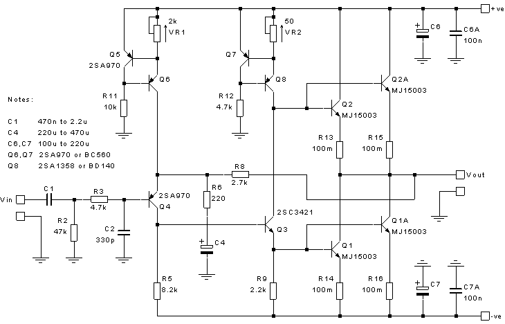
There are 2 variable resistor vr1 2k and vr2 50ohm.
Supply voltage is 24v.
According to guide Quiescent Current needs to be 3.7A.
There are 2 variable resistor vr1 2k and vr2 50ohm.
Supply voltage is 24v.
According to guide Quiescent Current needs to be 3.7A.
Member
Joined 2009
Paid Member
It should be pointed out that a resistor fed by a constant voltage source can be considered a constant current source.
The challenge comes because the resistor in question needs to have a constant voltage across it so even a constant voltage power supply is insufficient unless the other end of the resistor is also at a constant voltage. given that the JLH amplifier doesn’t have a constant voltage across both ends of the top resistor a constant voltage power supply doesn’t help. The bootstrap fixes this issue by holding the lower resistor at a constant voltage on both ends.
If you get into CCS theory it gets very weird. Best to say what we are doing with the everyday transistor amplifier.
Great myths have grown up between valves and transistors. Mostly not true. The great similarity is how they produce amplification. Biasing aside the output is not linear due to runing out of headroom to the supply voltage rail and impedence changes. In the end it hits the rail and the amplifier clips. A constant current source ( CCS ) fools the process somewhat. The colllector or anode sees a load which looks exactly like a resistor fed by a high voltage. If you imagine a rope between two points it's like we pull on it to make a more linear rope curve ( parabola or catenary, likely the latter if having minimal mass ). Just like the rope we can not make it 100% linear due to similar forces. The great advantage is we make a low voltage device more linear at lets say up to 90% maximum. It needs to be a voltage amplifier which mostly transistor amplifier stages are not to say this. JLH driver is a complex volatge amplifier. It has a bootstrap CCS. They are mostly equal as a linearity cure. A Cascode CCS is the most interesting if a small amount of headroom is available.
If the transistor amplifier has a longtail pair input stage ( JLH isn't ) the CCS assists in reducing PSU noise. It's a cheap upgrade. The PSU has to be very bad to prove it works. A resistor is faster although not in a meaningful way when audio.
I never did understand the JLH current settings fully as I was taught it couldn't work. My JLH did work so that is slightly wrong. I did notice if the heatsink slightly smaller it didn't work. Obvious, but not always said. On paper it should have worked.
potstip - a couple of points first. I take it this is each supply 24V (i.e. +/-24V) and intended for 4 ohm load?
You will need to be able to measure the current. A voltmeter with a 1V scale would be ideal as you could measure the voltage across one of the load sharing resistors (R13 or R15 for example).
Start with the 50ohm resistor at MAX. (I think the diagram is actually wrong because winding the pot clockwise (I take it upwards towards the + rail) increases the resistance. The wiper should be on the lower end).
VR1 (the 2k pot) should start in the middle.
I suggest this is an iterative process (I have never actually set one of these up!).
Start by setting the output rail to zero using VR1 (with no load). Should not need much trimming from centre, I'm guessing between 25 and 75% of the travel.
Then measure the voltage across one of the load sharing resistors, and slowly wind the 50 ohm pot down in resistance until you measure 185mV across it. That is 1.85A or half the quiescent current needed.
Then check the output centre rail voltage and trim again as the VAS current will cause an imbalance.
Lastly you can check that there is 185mV across all 4 emitter resistors to check uniformity.
I trust you have good heatsinks (45W per transistor will need at least 1C/W per device) and a suitable PSU. This is hot stuff.
I don't think this circuit is actually ideal. The two pots should have limiting resistors. In the case of the 50 ohm I would think 10 ohms suitable, but it maybe that some transistors will need more current, so 4.7 ohms might be needed. That would at least be 10% of the range and provide some degree of protection against inadvertently starting with zero ohms. Same for the 2k pot but here I suggest 470 ohms as a reasonable limiting value.
Last edited:
Hi Nigel
Here's one myth that is true - no complementary valve! Hence the use of transformers in nearly all OP stages. I've only ever seen one valve design with enough valves in parallel for direct coupling.
As for the JLH - it's simple. The bootstrap (= a pretend constant current) carries 2x the bias current needed for the output stage. Halfway down at the output rail it loses half into the upper output transistor and that leaves the rest to drive the lower OP transistor (apart from a leakage across the base resistor).
Since the bootstrap current is "constant" any current needed by the upper OP tranny is sucked out and whatever is left drives the lower device (at lower current). ANd vice versa. The driver transistor splits the current almost ideally between the two according to the demanded signals.
In maths terms Ib1+Ib2=constant. BUt these can be split in any way needed.
Hi Potstip -
NOte that VR1 is more likely to need to increase the resistance than lower if you start in the middle. It might be better to start at MAX resistance too. What is important is that you don't start at MIN.
Also when adjusting VR1 reducing the resistance lowers the output voltage, so if you like the clockwise pot direction to increase the output voltage the resistance should increase, so here the diagram is right.
Hi John a valve with a P type output holes in what looks like an anode. The old Philips TV output used a NPN NPN albeit valves and 800 ohms speaker. Not unlike a JLH in some ways.
My curiousity is about thermal stability. I don't remember my JLH drifting much. The heatsink was very large. If a class AB was set up this way it would drift a lot.
My curiousity is about thermal stability. I don't remember my JLH drifting much. The heatsink was very large. If a class AB was set up this way it would drift a lot.
Hi Nigel,
Many commented at the time the original article appeared that there was no thermal compensation. Yet, many hundreds (thousands?) of JLH 69's have been built without trouble. I suspect this is to do with the drive being current rather than voltage. The current gain does not vary as much with temperature compared with a Vbe (the standard -2mV/degC) and most Class AB designs use some form of voltage bias in the VAS, which itself is a current drive, and, coupled with a generally low dissipation in the devices means that unless the quiescent current bias system balances the Vbe(s), drift is significant.
So JLH's original design is remarkable in a number of ways.
THe downside was always that current driving with a limited reverse base current (on the lower device, only a 2k resistor) meant that the frequency response was limited by the fhfe of the transistors. In a class AB design, the drivers can source and sink current, so provide a wider bandwidth.
That's very interesting John and I suspect no one ever said that before. It makes perfect sense. As I said before slightly undersized heatsinks might show runaway. If they do reduce the current as it should give reasonable results. I guess the fixed mid voltage is a current reference. Happy to be wrong on that as I never truely understood it. Laziness mostly.
Yes, thermal runaway can still be a problem, but as long as people use big enough heatsinks the JLH seems stable. In the old days when RCA used to make transistors, their published data showed that the 2N3055 for example actually had an NTC of gain at a current of 1A or more. A more recent device like the MJ21194 shows similar - but only over 8A. Below 8A it has got a positive temp co so there would be more drift in a JLH.
Therefore, assuming devices are more like the 21194 these days it is important to use a heatsink large enough to prevent runaway with the expected change in gain with temperature.
Therefore, assuming devices are more like the 21194 these days it is important to use a heatsink large enough to prevent runaway with the expected change in gain with temperature.
That certainly helps too. In the original JLH specified MJ480's which have an increased in gain and like all transistors of that type and era a gain roll-off. The gain roll-off is almost compensated by the gain increase so not a guarantee.
The 2N3055 as published showed a lower gain at higher currents. If all devices were like the typical that assured thermal stability, whatever gain reduction would have assisted.
Not now, current 3055's are more like all of the commoner (older) epitaxial base transistors.
But it is probably the case that overheating is the problem with the JLH rather than runaway because of the limited current drive.
- Home
- Amplifiers
- Solid State
- JLH 10 Watt class A amplifier