Let's find the problem, first.
Indeed, fully agree John, that's the smart thing to do. Indiscriminate desoldering of everything three-legged seems a bit daft.
Jan
What I meant to say, Joshua, is that we should find and fix the problem first. It would be best, if the jfets are OK, because it will be somewhat difficult to replace them, as we will probably have to double up to create an approximation of the original part. Idss is the most important thing and it can be measured with a 10 ohm resistor, a 9V battery and a voltmeter. You just measure the current across the resistor. In fact, with a current reading meter, you don't even need the 10 ohm resistor. Just put the middle pin (gate) to one other pin (source or drain, they are symmetrical) and put the 2 leads to one side of the 9V battery, and connect the other terminal of the 9V battery to the single lead that is left. Battery polarity will depend on whether the fet is N channel or P channel. That is all there is to it. Get Idss right and Gm will be predictable and close to the complementary device. There is no need to worry over anything else until the unit gets fixed.
Yeah, lots of possibilities. Damaged caps come to mind. Sloothing out noise can be difficult sometimes.
Last edited:
Joshua, quit worrying and let's fix your preamp.
Hi John,
Thank you.
I don't worry at all, I'm waiting for the components to arrive so that I'll be able to fix the preamp. Till then, I'm contemplating options…
I have endless curiosity both about electronics and about what affects sound quality.
Using N JFETs instead of P ones in such a circuit wouldn't work for the sole reason that N ones require negative bias, while P ones require positive bias.
Anyhow I'd be glad to know how to practically attain matching forward gain between N & P devices in various circuits, especially in the one I have.
Indeed, fully agree John, that's the smart thing to do. Indiscriminate desoldering of everything three-legged seems a bit daft.
Jan
Hi Jan,
Thank you.
I have no intention to remove the FETs from the PCB, unless nothing else will work.
What I meant to say, Joshua, is that we should find and fix the problem first. It would be best, if the jfets are OK, because it will be somewhat difficult to replace them, as we will probably have to double up to create an approximation of the original part. Idss is the most important thing and it can be measured with a 10 ohm resistor, a 9V battery and a voltmeter. You just measure the current across the resistor. In fact, with a current reading meter, you don't even need the 10 ohm resistor. Just put the middle pin (gate) to one other pin (source or drain, they are symmetrical) and put the 2 leads to one side of the 9V battery, and connect the other terminal of the 9V battery to the single lead that is left. Battery polarity will depend on whether the fet is N channel or P channel. That is all there is to it. Get Idss right and Gm will be predictable and close to the complementary device. There is no need to worry over anything else until the unit gets fixed.
Hi John,
Thank you.
Again, I have no worries.
As I wrote previously, all the relevant capacitors will be replaced and PCBs cleaned first. The capacitors (and rectifying diodes and PSU snubbers) will be here in about a week time.
Should there still be noise, I'll try to pinpoint the noisy devices, both with freeze spray and with a scope. Should any FET be noisy, I'll replace N-P arms with 2 parallel N and 2 parallel P, BL grade devices. Should I wouldn't succeed in pinpointing the noisy ones, Ill replace all of them.
Pondering about matching forward gain is mainly out of my quest for better electronics knowledge. However, should I figure it out, it may be of a practical benefit as well. I do know that no design and no circuit are perfect, none can be perfect. However I'd be very happy getting better results, if and when practically possible.
I know how to measure Idss.
Yeah, lots of possibilities. Damaged caps come to mind. Sloothing out noise can be difficult sometimes.
Hi John,
Thank you.
With more than 45 years of experience in repairing electronic circuits; audio, video, TV and RF; in consumer and professional gear; I'm absolutely confident that I'll manage removing the noise completely.
However it doesn't stop me from consulting here.
Joshua:
Patrick (Euvl) has shown some results of applying slightly mismatched source degeneration resistors and selecting slightly mismatched Idss to help out with transconductance difference between N & P jfets if you have concerns about it. I think it's in his thread on a balanced F5 design?
mlloyd1
Thanks Joshua's description is almost exactly what I found in simulation, but this probably just confuses the issue until the preamp is working again.
The significant source degeneration of each part tends to make absolute matching for Gm less useful.
Thanks Joshua's description is almost exactly what I found in simulation, but this probably just confuses the issue until the preamp is working again.
Hi Scott,
It means that your models are quite accurate, at least regarding gm. I'd love to see your models, regardless of whether I'll use it in repairing this stage, or not.
The significant source degeneration of each part tends to make absolute matching for Gm less useful.
Thanks, John.
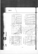

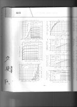
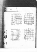
These are really quite primitive actually but do predict basic biasing and differences well enough. You just take the plot from the datasheet and do a fit to gm = 2*sqrt(beta*Id) gets close enough.
.model 2sj74 pjf
vto = -sqrt(idss_p/beta),beta = .051,lambda = 10e-3,cgs = 105.0pf,cgd = 105.0pf,pb = .6,mjd = .5,mjs = .5
.model 2sk170 njf
vto = -sqrt(idss_n/beta),beta = .043,lambda = 10e-3,cgs = 30.0pf,cgd = 30.0pf,pb = .6,mjd = .5,mjs = .5
lambda is hard to read off the datasheet usually only matters a little so this is just a space holder/estimate.
vto is shown as the formula, you need to fill in the value for your idss.
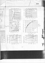
This is where my style of design is somewhat different from many other designers. I don't use a computer model, I use the graphs from the data sheets.
These are really quite primitive actually but do predict basic biasing and differences well enough. You just take the plot from the datasheet and do a fit to gm = 2*sqrt(beta*Id) gets close enough.
.model 2sj74 pjf
vto = -sqrt(idss_p/beta),beta = .051,lambda = 10e-3,cgs = 105.0pf,cgd = 105.0pf,pb = .6,mjd = .5,mjs = .5
.model 2sk170 njf
vto = -sqrt(idss_n/beta),beta = .043,lambda = 10e-3,cgs = 30.0pf,cgd = 30.0pf,pb = .6,mjd = .5,mjs = .5
lambda is hard to read off the datasheet usually only matters a little so this is just a space holder/estimate.
vto is shown as the formula, you need to fill in the value for your idss.
Hi Scott,
Thank you very much.
I'll play with some simulations on the circuits I have. I'll double the devices in the schematic, as it will actually be if I'll need to replace JFETs.
The simulation will be used only to estimate matching forward gain between N & P pairs. I don't trust simulations much, especially when the models aren't given by the manufacturer.
Your models allow me to simulate devices of any Idss. All other models I've seen so far where for only 1 given Idss.
However, a quick glance at the models shows that beta is different between the 2 devices, and therefore also vto is different.
This is where my style of design is somewhat different from many other designers. I don't use a computer model, I use the graphs from the data sheets.
Hi John,
It looks to me like you managed to have some very successful designs, so using computer models my not be the key to successful design… 🙂
There is one problem with computer designed circuits that stands out to me, and that is the MODELS of jfets are not as accurate as I would want. Now, I come from the 'slide rule' generation, so I learned electronic design before everybody had their own personal computer, so I had to read the graphs, and learn alternative design techniques. Back at the beginning of Spice for mainframe computers I was exposed to the models and even had a Spice program run with one of my jfet designs, with disappointing results. The potential was there, but the models were not good enough. This is not to discourage use of LT Spice for circuit modeling. I wish I could run Spice, myself, but it has not been absolutely necessary for the sort of designs that I do.
- Status
- Not open for further replies.
- Home
- Source & Line
- Analogue Source
- JFETs replacing and matching questions