In my view,
as long as the the bass is firm enough, a higher output impedance is advantageous for linearity. I`m suspicious about an accentuated brightness, a sign of high frequency disorder. Listening fatigue indicates grave phase errors.
This seems to contradict evrything i have heard. Let's say you have a biamped system with a FR on top and helper woofer. You are saying that a high output impedance would be better for the FR? At what point is the output impedance too high? Should you match to your driver? Any guidance or theories on making this decision?
Member
Joined 2009
Paid Member
Harmonic distortion does not cause listening fatigue.
it must be user dependent then, because I get fatigued listening to excessive distortion

Guys, do not take too serious what I said about difference between jFET and RF MOSFET versions, the difference is really very small, it has nothing to do with difference relative to Class D.
I speak about subtle difference, similar to the effects of burning-in, at the level of slight personal preference. And in my feeling the MOSFET version is perfect, I simply wonder why others prefer jFET nevertheless.
As for phase shifts, in both cases they are very small, visible shift between input and output sine waves only at 1 MHz. THD of the source follower also has no reason for troubles.
buzzforb,
in principle, the output impedance could be very high, the purpose of a low output impedance is to provide damping. My feeling is that FR speakers are suitable for being driven by a high impedance source. I don`t expect problems with the frequency response, not sure regarding damping in the low frequency range though.
FR speakers produce a homogeneous sound stage that has dimensions, a natural sound without listening fatigue.
Hi,
the decent conventional biasing method, whereby the voltage is directly applied to the gate and source is not in need of improvement. Reverse bias gives linearity. Acting as a voltage source, the series pass device should be bipolar. (Shall we call it the poor man`s choke?)
the decent conventional biasing method, whereby the voltage is directly applied to the gate and source is not in need of improvement. Reverse bias gives linearity. Acting as a voltage source, the series pass device should be bipolar. (Shall we call it the poor man`s choke?)
Attachments
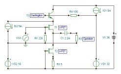
This is another version of ground referencing and load connection.
People noted that in this version an influence of the output caps C3 and C4 is additionally diminished.
In this version, EMF of distortions from electrolytics do not sum up directly with output signal, instead, it is applied to the drain of the active device and act as power rail distortions. Active device suppresses it partially.
Attachments
Last edited:
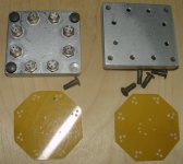
This is my next step to more powerful jFET, cluster of 8pcs matched KP903A.
Idss is close to 4A, Ciss less than 200pF. It is planned for using with 2,5A idle current.
The heat is spreaded by 12mm aluminium slab, the screws are from non-magnetic material (titanium).
New buffer will be probably extended by front-end amplification stages, and probably current NFB will be added for achieving Zout less than 0,1 Ohms.
Attachments
Last edited:
What will the circuit board material be used for? Looks like you screwed in the JFETs and then drilled the circuit board material to match where the pins ended up after tightening them into the aluminum slab.
se
se
What will the circuit board material be used for? Looks like you screwed in the JFETs and then drilled the circuit board material to match where the pins ended up after tightening them into the aluminum slab.
se
Hello, Steve
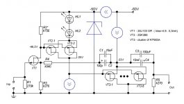
I used standard PCB material, glass fiber plastic. It is not copper plated, just a plastic. I did p-to-point wiring (monowire in teflon), then put teflon circle over the wires, and gate stopper resistors over it.
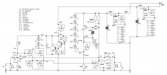
Here I enclose shots of the assembled devices, and some measurement results.
Working point is planned at Id=2,2A, Vgs=-2,4V. Linearity around the working point is very good, although transconductance at this point is near 0,7S only, not so high.
Therefore, using of some NFB for decreasing Zout could be desired.
Attachments


Last edited:
you can pull right side of R4 to output node
in that case leave C1 , C2 out 😉
Yes, good proposal, however, in this case we have voltage amplification around 20...30, and, correspondingly, Zout of this version will be 10 times higher.
Attachments
Yes, good proposal, however, in this case we have voltage amplification around 20...30, and, correspondingly, Zout of this version will be 10 times higher.
.........
mea culpa - I meant like this , but forgot on source potential .......... 😉
Attachments
Last edited:
.........
mea culpa - I meant like this , but forgot on source potential .......... 😉
This version is also attractive, it will need removal of R5.
And, from my previous experience with Zen9, taking the NFB after output cap, although theoretically attractive (cap distorsions are suppressed), cuases unfavourable electromagnetic interactions, and makes difficult (additional correction needed) to have a nice square-wave responce.
At the moment, I would prefer your previous version, it is suitable for integrated amp, and Zout can be close to 0,1 Ohms.
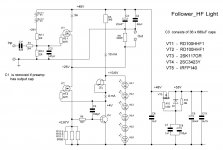
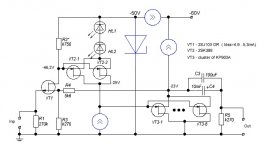
This is an implementation of the draft schematics into more detailed schematics layout.
I hope that using 2SK389 as VT2, VT3 will ensure thermal stability, that is usually a problem with CCS-like load. If it is not the case, than resistive load will be used.
I hope that using 2SK389 as VT2, VT3 will ensure thermal stability, that is usually a problem with CCS-like load. If it is not the case, than resistive load will be used.
Attachments
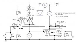
Why do you twist it upside down...??
now the reference is no longer the regulated postoperative rail...but the GND...??
now the reference is no longer the regulated postoperative rail...but the GND...??
Why do you twist it upside down...??
now the reference is no longer the regulated postoperative rail...but the GND...??
Yes, I made the schematics more close to standard form (ground is at the bottom).
I have been advised to do so, since custom is a big force.
I hope, it will be a high quality integrated amp.
but your GND is now directly connected to the main PSU and transformer....the purety in the previous was that the CCS shielded the GND or low voltage ans the higher rail was regulated..So you by those choices took the PSU effectively out of the loop.. Now you put them back in..??
- Status
- Not open for further replies.
- Home
- Amplifiers
- Solid State
- jFET Power Buffer