Nice mikelm, wish I had thought to use those little pins - makes part swapping much easier!
yeah, but the soldering beneath it will easily be 'boiled'
easier to just flip the board, copper facing up
I'm thinking on using a non copper perforated board. I already have the pins and a small piece of board. I never thought of combining the two.
I will go and check how tight a fit the pins are in the holes I have.
I will go and check how tight a fit the pins are in the holes I have.
Yeessss.
One end of the pin is smaller in diameter and it is a slack push fit. This end has some rifling and when pushed home becomes a tighter fit.
The other end of the pin is slightly larger and it is a tight push fit (pliers probably) for a more secure fitting of pin to perf board.
One end of the pin is smaller in diameter and it is a slack push fit. This end has some rifling and when pushed home becomes a tighter fit.
The other end of the pin is slightly larger and it is a tight push fit (pliers probably) for a more secure fitting of pin to perf board.
easier to just flip the board, copper facing up
No copper - it's plain board
I was thinking about different gate stoppers...due to different input capacitance (Ciss)...of the output laterals...one is 500p (N) the (P) has 700 p...So in order to have similar capacitance one could add 200p over the N or have different resistors to the gate to have the same drive of the FET...
I do think that adding some capacitance could prove to be the best solution.. or..?? (knepper vi fluer..??) sorry can't translate that....🙂
I do think that adding some capacitance could prove to be the best solution.. or..?? (knepper vi fluer..??) sorry can't translate that....🙂
In simulation I used 350R on the N and 220R on the P. This gave equal response time for both.
The capacitances vary nonlinearly with voltage, so adding capacitance to one to even them out will only really work at low signal levels. Same with different gate stoppers.
- keantoken
The capacitances vary nonlinearly with voltage, so adding capacitance to one to even them out will only really work at low signal levels. Same with different gate stoppers.
- keantoken
Wouldn't be better to reduce the gatestoppers by a factor 10 and move the generated phaseshift a decade up.
The gatestoppers is there mainly because of the wire inductance.
they would then nearly be in parallel and will not entirely but close balance the capacitance change out.
I would bet some poweramp pcb to greg and hugh that it should work with the reduction of the gatestoppers.
The gatestoppers is there mainly because of the wire inductance.
they would then nearly be in parallel and will not entirely but close balance the capacitance change out.
I would bet some poweramp pcb to greg and hugh that it should work with the reduction of the gatestoppers.
Yes. I have worked with fets before. 220r will slow down the transition time. Regardless If we talk class d pr turn off/turn on time when moving from conducting to non conducting in class ab or b
It works fine with 200R gate stoppers, as I have used in my previous schematics. I just put the 500R ones there on the last version because I was experimenting to get rid of the oscillation. As it turns out, it was the vas gate stopper, not the output gate stoppers that was the problem.
It works fine with 200R gate stoppers, as I have used in my previous schematics. I just put the 500R ones there on the last version because I was experimenting to get rid of the oscillation. As it turns out, it was the vas gate stopper, not the output gate stoppers that was the problem.
ok, have you tried to lower the values on the output mosfet? but again if it works fine there is no reason to change them.
As hugh writes: how does it sound? Its allways the most exciting point. You can test and sim, but it does not tell you anything about the sound..
I've already commented on how it sounds, let's wait to see what mikelm thinks.
In the meantime, let me say it sounds as it simulates. Plenty of drive, clean treble, a pronounced midrange and punchy bass. Plenty of detail without being clinical. 9610 version is a little warmer sounding. At least this is in my opinion with my speakers.
As i am on holiday all my writing is currently being done on my phone which makes a longer response tiresome. I will write more when I return, but I am hoping mikelm will beat me to it.
100w into 8ohms load
to lineup,
was the 100w into 8ohms load [post#9] your final take on the Fetzilla design? I'm begining to have an interest...
to lineup,
was the 100w into 8ohms load [post#9] your final take on the Fetzilla design? I'm begining to have an interest...
Hi all,
I will post a schematic once I'm back unless Hugh beats me to it.
Hello swordfishy and Hugh
Is there a phase lead capacitor in the final schematic ?
Thank
Bye
Gaetan
No, Gaetan,
BUT, we have left provision for it on the pcb so people can experiment.
Welcome back to the thread!
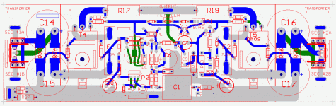
Revised pcb, with ZVP2210 2W FET VAS in place, attached. There is also provision to cut the pcb along two vertical lines just inside the power caps to permit an outboard power supply (note two spade connector locations).
Hugh
BUT, we have left provision for it on the pcb so people can experiment.
Welcome back to the thread!
Revised pcb, with ZVP2210 2W FET VAS in place, attached. There is also provision to cut the pcb along two vertical lines just inside the power caps to permit an outboard power supply (note two spade connector locations).
Hugh
Attachments
No, Gaetan,
BUT, we have left provision for it on the pcb so people can experiment.
Welcome back to the thread!
Revised pcb, with ZVP2210 2W FET VAS in place, attached. There is also provision to cut the pcb along two vertical lines just inside the power caps to permit an outboard power supply (note two spade connector locations).
Hugh
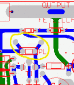
Hello Hugh
I think I found where is the place for experimenting a phase lead capacitor on you pcb.
Is it where I've put a yellow circle in my pcb image ?
Thank
Bye
Gaetan
Attachments
- Status
- Not open for further replies.
- Home
- Amplifiers
- Solid State
- JFET input, MOSFET VAS, LATERAL output = Perfect!!