Can any FET experts help me here?
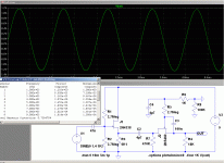
I am trying to knock up a very simple FET buffer that incorporates a click-less mute switch on the output. This circuit is to be used for a general purpose unbalanced audio input box for a PA system, where the input can be silenced if necessary without any “pop” or clicks. The input impedance needs to be 1 Meg Ohm and the output impedance as low as possible, the sound quality needs to be as high as possible, and the power source needs to be a single 9V battery with as long a life as possible (conflicting requirements probably)
So far, I have the circuit below which functions and sounds good before the switching section (at C2 negative), but after the switch the sound looses a tiny bit of clarity and “life” if you know what I mean. The muting function works quite well, and this is achieved by disconnecting the D4 from Ground.
Can any of you guys and girls suggest what I can do or change to improve this circuit as to be honest I have no idea if the component values I have in the switching circuit are correct for good sound quality?! The FETs used are the only ones I have available unfortunately and so I would like to use these if at all possible. I know that my aims can be easily achieved using op-amps and CMOS switches etc, but I like the simplicity, low power requirement, and “sound” of the FET buffer and so I would like to stick with it. The circuit needs to drive a 20Kohm mixer input impedance.
Hope you can help me and thanks
Ray
I am trying to knock up a very simple FET buffer that incorporates a click-less mute switch on the output. This circuit is to be used for a general purpose unbalanced audio input box for a PA system, where the input can be silenced if necessary without any “pop” or clicks. The input impedance needs to be 1 Meg Ohm and the output impedance as low as possible, the sound quality needs to be as high as possible, and the power source needs to be a single 9V battery with as long a life as possible (conflicting requirements probably)
So far, I have the circuit below which functions and sounds good before the switching section (at C2 negative), but after the switch the sound looses a tiny bit of clarity and “life” if you know what I mean. The muting function works quite well, and this is achieved by disconnecting the D4 from Ground.
Can any of you guys and girls suggest what I can do or change to improve this circuit as to be honest I have no idea if the component values I have in the switching circuit are correct for good sound quality?! The FETs used are the only ones I have available unfortunately and so I would like to use these if at all possible. I know that my aims can be easily achieved using op-amps and CMOS switches etc, but I like the simplicity, low power requirement, and “sound” of the FET buffer and so I would like to stick with it. The circuit needs to drive a 20Kohm mixer input impedance.
An externally hosted image should be here but it was not working when we last tested it.
Hope you can help me and thanks
Ray
The key to make a JFET switch work is to have the gate track the voltage of the source in the on-state. The gate drive circuits needs some changes. Here's what you need: www.seekic.com/uploadfile/ic-circuit/200963021645243.gif
Also you might want to consider paralleling some 2N5460 to lower the effective on-resistance. No matching needed.
Samuel
Also you might want to consider paralleling some 2N5460 to lower the effective on-resistance. No matching needed.
Samuel
Why are you running the signal through the FET? You can accomplish the same goal by having the FET in shunt, shorting the output to ground until enough voltage builds up on the FET gate to cut it off.
Sam
Thanks for your time and help, much appreciated!
I have modified the switch circuit to your suggestion and added another FET in parallel and this seems to work very well in simulation with over half the distortion I was getting before! As soon as I get the time I will bread board it and see if my sound has improved and see if the mute is nice and smooth. I'll let you know as soon as can
Sy
Thanks for your reply and time also! To be honest my friend, I chose the series circuit as there are examples on the net that I can try, although none have worked as well as Sam's suggestion. Shunt seems to make good sense but my electronics knowledge is not up to figuring out the circuit, although I have learned a great deal from you guys already!
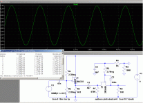
Do you guys think the component values I have around the FETs in the circuit below are OK for a stable and reliable circuit?
Cheers
Ray
Thanks for your time and help, much appreciated!
I have modified the switch circuit to your suggestion and added another FET in parallel and this seems to work very well in simulation with over half the distortion I was getting before! As soon as I get the time I will bread board it and see if my sound has improved and see if the mute is nice and smooth. I'll let you know as soon as can
Sy
Thanks for your reply and time also! To be honest my friend, I chose the series circuit as there are examples on the net that I can try, although none have worked as well as Sam's suggestion. Shunt seems to make good sense but my electronics knowledge is not up to figuring out the circuit, although I have learned a great deal from you guys already!
Do you guys think the component values I have around the FETs in the circuit below are OK for a stable and reliable circuit?
An externally hosted image should be here but it was not working when we last tested it.
Cheers
Ray
Missed something in my first post. I think you should move C2 between the drain of J2/J3 and R9 (I presume R8 just models the mixer--otherwise you could skip it). Otherwise sufficiently negative voltage swing will turn on D4. R2 is not needed then, and R10/R12 could be made about 10x lower which should bring HF distortion down a bit. Also between C7 and V+ there should be a resistor to define the time constant.
I don't think a shunt switch will work particularly well here. To make it effective we a need significant source impedance, which is no what we want here.
Samuel
I don't think a shunt switch will work particularly well here. To make it effective we a need significant source impedance, which is no what we want here.
Samuel
Thanks Sam!
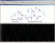
I altered the circuit to below as I think you suggested, and although it improved the on performance a little (a little less distortion) when on, the muting action does not seem to be as good or working. When muted it seems to cut positive swings completely but lets about 12mV through on negative swings. If the input is increased to about 1.0vrms then the positive peaks get let through by about 450mV rms. The resistor for the RC time constant seems to have no effect when set to about 5mSecs with 1K (I think!)
I have also attached the files just in case you have LTspice
Can you help?
Cheers
RayView attachment 209627
I altered the circuit to below as I think you suggested, and although it improved the on performance a little (a little less distortion) when on, the muting action does not seem to be as good or working. When muted it seems to cut positive swings completely but lets about 12mV through on negative swings. If the input is increased to about 1.0vrms then the positive peaks get let through by about 450mV rms. The resistor for the RC time constant seems to have no effect when set to about 5mSecs with 1K (I think!)
An externally hosted image should be here but it was not working when we last tested it.
I have also attached the files just in case you have LTspice
Can you help?
Cheers
RayView attachment 209627
Attachments
I think it has to do with the offset at J1 source. Let's simplify and temporarily replace R7 with a current source of desired value--at least 1 mA I'd say. Then adjust R4/R5 such that the source of J1 sits at about 4.5 V. How does off-state headroom look now? The actual optimum operating point will be somewhat different from 4.5 V, but also dependent on the actual transistor parameters, mostly Vp.
Samuel
Samuel
The value of R7 (6.1K) was found using the actual J201 I have in the circuit. I just scoped up the output of the buffer (minus the switch circuit) with a 1 kHz input and adjusted a 10K pot in place of R7 to enable the largest signal input without any sign of clipping. This finally measured the 6.1K used in the sim. The J201 model in LTspice is probably not the same. I checked the J201 model and found the Idss is 594.1uA and Vgs-off is -600.4mV incidentally
With the circuit as my last post, the waveform at the output with the circuit muted and a 0.25Vrms input is as below
and with a 1.0Vrms input it looks like this
I swapped R7 out for a DC current source of 1.0mA and adjusted R4 to 2.47MEG Ohms to set the quiescent voltage at J1 source of 4.5V and the resulting muted output changed to the below with a 0.25Vrms input
and with a 1.0Vrms input it looks like this
Does this shed any light on the issue?
Once again thanks for all your time and help Sam, very much appreciated!!
Cheers
Ray
With the circuit as my last post, the waveform at the output with the circuit muted and a 0.25Vrms input is as below
An externally hosted image should be here but it was not working when we last tested it.
and with a 1.0Vrms input it looks like this
An externally hosted image should be here but it was not working when we last tested it.
I swapped R7 out for a DC current source of 1.0mA and adjusted R4 to 2.47MEG Ohms to set the quiescent voltage at J1 source of 4.5V and the resulting muted output changed to the below with a 0.25Vrms input
An externally hosted image should be here but it was not working when we last tested it.
and with a 1.0Vrms input it looks like this
An externally hosted image should be here but it was not working when we last tested it.
Does this shed any light on the issue?
Once again thanks for all your time and help Sam, very much appreciated!!
Cheers
Ray
Here is a possibility (the 2N4438 is identical to the J201).
There is some distortion in the ON state, but it is caused by the follower, not by the switch: the upstream signal is shown for reference and has similar distortion (a shade higher in fact).
There is some distortion in the ON state, but it is caused by the follower, not by the switch: the upstream signal is shown for reference and has similar distortion (a shade higher in fact).
Attachments
Hi Elvee!
Thanks for your help my friend!
The J201 model I am using is as follows:
.MODEL J201 NJF(Beta=1.621m Betatce=-500m Rd=1 Rs=1 Lambda=2.236m Vto=-600m Vtotc=-2.5m Is=114.5f Isr=1.091p N=1 Nr=2 Xti=3 Alpha=506.8u Vk=251.7 Cgd=4.667p M=227.1m Pb=500m Fc=500m Cgs=2.992p Kf=0.6042f Af=1)
The input condition of 1Vrms is probably the maximum the unit will ever see and the majority of the time the input signal will be less than 0.5Vpk and therefore I think the distortion figures will be acceptable, as this unit will not be used for recording applications or similar. Using a J201, the sound from the buffer only is very good and I was pleased with the results. When the required muting action circuit was added, the sound suffered a little in clarity and seem to lose it’s “edge” (no doubt caused by the additional distortion that my circuit errors had introduced) and hence why I came to you guys for help.
Sam's suggested circuit changes seem to be working well in simulation and when the mute is off, the output THD is around 0.5% or so with 1Vrms input and around 0.1% for 0.5Vpk input, both figures are a big improvement. It is just a case of getting the circuit to mute quietly and reliably which is causing a few headaches right now! Unfortunately, I am now a little out of my depth with FET circuit theory and so I am at your mercy!!
Cheers
Ray
Have a read of Pass B1 buffer.
When you have downloaded and fully understood that pdf, you will be much better placed to make desicions on your own follower.
Worth looking at the BF862 follower and amplifier threads.
When you have downloaded and fully understood that pdf, you will be much better placed to make desicions on your own follower.
Worth looking at the BF862 follower and amplifier threads.
Don't have any acess to SPICE software at the moment, unfortunately. Ray, could you post a graph which shows gate, drain and source voltage of J2 (of your latest schematic with my suggested circuit)? That is with about 1 Vrms drive and off state.
Samuel
Samuel
Hi Sam
No Problems! Here is the circuit with the CC in J1 Source and R4 adjusted to give 4.5V quiescent at the Source
Here are the resulting waveforms with the circuit muted...
V(n002) = J2 Drain (left of FET)
V(n003) = J2 Source (right of FET)
V(n007) = J2 Gate
Does this help?
Thanks for the pointer there Andrew, appreciated. I did actually look over this circuit before settling on the simple version I have. I was not sure if it would be suitable for a 9V supply and high input impedance. I also didn't really want to get into matching FETS etc (I know, lazy!!) as I only have a few of the devices. The sound and performance of the buffer itself is pretty good and therefore my main concern is the mute switch at present. However the B1 circuit looks very interesting and comes from a very highly respected source and so I am sure I will play around with this as well!
Thanks all
Ray
No Problems! Here is the circuit with the CC in J1 Source and R4 adjusted to give 4.5V quiescent at the Source
An externally hosted image should be here but it was not working when we last tested it.
Here are the resulting waveforms with the circuit muted...
V(n002) = J2 Drain (left of FET)
V(n003) = J2 Source (right of FET)
V(n007) = J2 Gate
An externally hosted image should be here but it was not working when we last tested it.
Does this help?
Thanks for the pointer there Andrew, appreciated. I did actually look over this circuit before settling on the simple version I have. I was not sure if it would be suitable for a 9V supply and high input impedance. I also didn't really want to get into matching FETS etc (I know, lazy!!) as I only have a few of the devices. The sound and performance of the buffer itself is pretty good and therefore my main concern is the mute switch at present. However the B1 circuit looks very interesting and comes from a very highly respected source and so I am sure I will play around with this as well!
Thanks all
Ray
Thanks. V(n002) is the source, not drain, right?
So let's adjust R4/R5 to give a quiescent output of about 3 V. How do things look now?
You probably won't get around selecting 2N5460s for low Vp if we stick with this basic idea. I do have some others, but it will take a couple of days till I can post these.
Samuel
So let's adjust R4/R5 to give a quiescent output of about 3 V. How do things look now?
You probably won't get around selecting 2N5460s for low Vp if we stick with this basic idea. I do have some others, but it will take a couple of days till I can post these.
Samuel
The B1 does not need matched jFETs.
It is far simpler than your version, it does not need any expertise to select resistor values.
But, I am not suggesting you build the B!. I am saying read about it and understand it. Then you could have sufficient knowledge to allow you to start "designing" your buffer.
Asking a simulator questions about a model is not designing if a.) you don't know what questions to ask and b.) you don't understand how to interpret the answers.
The B1 does not need matched JFETs.
If the JFET used as current generator has substantially higher Idss than the one used as source follower the circuit won't work. The JFETs may not need to be matched, but at least selected.
For good reading on JFET buffers see www.analogzone.com/col_01302004.pdf
But let's fix the switch first...
Samuel
Hi Sam
Thanks buddy! OK I adjusted R4 to hit 3.0V at J1 source. And the resulting circuit looks like this. I have hopefully clarified what I thought was the Drain, Source and Gate on J2 but I could be wrong!
And here are the resulting waveforms with clarification as to where they were measured...
The output is still not muted in this condition. I feared that the FETs I have available may not be suitable. Is there any way I could press another J201 in to switching service if the P type turns out to be no good?
Thanks Andrew. You are absolutely right; A little knowledge is often a dangerous thing! Unfortunately my knowledge is sketchy and this is why I turned to you guys for help. I am learning however, and Sams time and help is invaluable here and very much appreciated!
Cheers
Ray
Thanks buddy! OK I adjusted R4 to hit 3.0V at J1 source. And the resulting circuit looks like this. I have hopefully clarified what I thought was the Drain, Source and Gate on J2 but I could be wrong!
An externally hosted image should be here but it was not working when we last tested it.
And here are the resulting waveforms with clarification as to where they were measured...
An externally hosted image should be here but it was not working when we last tested it.
The output is still not muted in this condition. I feared that the FETs I have available may not be suitable. Is there any way I could press another J201 in to switching service if the P type turns out to be no good?
Thanks Andrew. You are absolutely right; A little knowledge is often a dangerous thing! Unfortunately my knowledge is sketchy and this is why I turned to you guys for help. I am learning however, and Sams time and help is invaluable here and very much appreciated!
Cheers
Ray
The output is still not muted in this condition. I feared that the FETs I have available may not be suitable. Is there any way I could press another J201 in to switching service if the P type turns out to be no good?
What's wrong with the solution of #9?
I have hopefully clarified what I thought was the Drain, Source and Gate on J2 but I could be wrong!
You are 😉. Source is the port closer to the gate in the symbol. See e.g. JFET - Wikipedia, the free encyclopedia
I feared that the FETs I have available may not be suitable.
Basically to have the FET in a high-impedance state, the gate must be more than Vp above the source voltage (for a P-channel). I think your 2N5460 model has a bit high Vp. Just to make sure that I'm not missing something more fundamental check if muting gets good if you bias the switching FET off with +20 V instead of +9 V.
Is there any way I could press another J201 in to switching service if the P type turns out to be no good?
That would have been my next suggestion. With these low supply voltages we just need parts with low Vp, and the J201 is a near-perfect example for such.
The solution is simple: keep the buffer, but power it from -9 V instead of +9 V. In other words: R5/I1 go to -9 V, R4 and J1 drain to ground.
-9 V is now the off bias point for the switch--turn D4 around.
What's wrong with the solution of #9?
It's basically a very interesting approach; however I fear that the switching time will be a bit high (~1 s for full mute). During on-to-off or off-to-on transition the signal might be seriously distorted, which becomes audible at such long transition times. Can R5 be reduced to something like 100k without compromising on-performance?
Samuel
- Status
- Not open for further replies.
- Home
- Amplifiers
- Solid State
- JFET experts needed!