I've been reading through this thread and it's been really interesting. Haven't built anything yet. Still need to source the jfets and need to finish one or two other projects first, but... I did use this as the source for teaching myself the basics of LT Spice and Eagle.
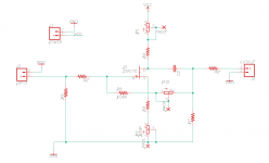
So I drew up a basic board in Eagle, then got the idea, inspired by some of the circuit variations here, to draw up an experimenter's variation of the schematic and PCB. The idea being to include the space for discrete resistors, trimpots, and the feedback traces, with room to jump off to daughter boards if you wanted to get fancy or just jumper or leave off what you don't want to use.
If you guys wouldn't mind sanity checking this and giving some feedback, I'd appreciate it. I think most of it is correct, but I'm not confident I got the trimpots drawn correctly. Note that this is just one channel at this time.
Is this even a useful idea?
BTW I know there definitely needs to be more space for the output cap on this board.
Thanks
Attachments
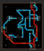
Looks unnecessary complicated and if you go 2 Layer route, I would make GND Plane.
Will you etch the PCB yourself?
Maybe for such a simple circuit P2P will be a good idea too?
Will you etch the PCB yourself?
Maybe for such a simple circuit P2P will be a good idea too?
There is a ground plane that I left out of the image for clarity.
I have etched my own in the past. Given the price and speed of PCB fab services today I no longer bother with keeping such chemicals around the house.
I have etched my own in the past. Given the price and speed of PCB fab services today I no longer bother with keeping such chemicals around the house.
Looks unnecessary complicated..
Only in this forum could a single transistor circuit be called that.
😛
I would suggest dragging components around to see how the tracks change and you will find many pleasant surprises.
For starters, without relocating (with respect to other components), see what happens
if you push C1 to the right, move R4 up to line up with trace N$5, drop the trace to R1 from R4 so it's vertical, rotate J2 90 degrees clockwise ...
I always liked Eagle much more than Kicad from this perspective. You'll find that you can easily make this board with 1/2 the space and have more direct traces at the same time.
Have fun with it!
twitchie, thanks for the tips.
For the record, this version of the board I created intentionally has a bit of extra room on it to make space for breaking out experimental additions. Like, say you wanted to try the CCS modification yggdrasil suggested (back in post 525 or thereabouts). You could simply jumper in a daughterboard. I actually imagined using right angle pins and plugging it in like a PC card.
Likewise, the pots enable tweaking source, drain and feedback resistors, but could easily be jumpered.
With a couple more components and a different transistor trace you could even build a regular BOZ on here I think.
I made another much smaller variation of this board, without accommodation for trimpots, though twitchie's suggestions made me realize it needs further tweaks also.
Very much digging Eagle. It's got a bit of a learning curve, and terrible documentation, but enough information out in the world to get started. The Sparkfun tutorials are very good.
Very much digging Eagle. It's got a bit of a learning curve, and terrible documentation, but enough information out in the world to get started. The Sparkfun tutorials are very good.
It is not going easyer than this 😀
Only in this forum could a single transistor circuit be called that.
😛
Attachments

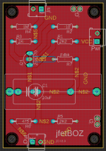
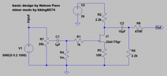
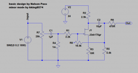
Thanks again for the feedback on my board. I've tossed out the adjust-anything idea and gone back to my first, simple, single-channel board. Made some changes to:
This version shows the ground planes as well. For scale, the outer cap pads are sized for a 37.5mm poly box cap, such as Wima MKP.
It looks right to me, but sanity check and comments welcome.
My biggest question is the best way to route a trace from the feedback resistor to the gate. It it better to have a shorter trace that cuts across Vcc input to drain via R1, or a longer route to the R3-Q1 trace, but that also cuts perpendicularly across the drain-C1 trace?
Oh, maybe I flip C1 and all of the feedback loop stays on the left side of the board, crossing nothing?
How do you approach layout issues like this?
This is how I learn.
Thanks
- make tracks less convoluted
- incorporate an optional feedback resistor
- allow space for various sizes of likely output caps
This version shows the ground planes as well. For scale, the outer cap pads are sized for a 37.5mm poly box cap, such as Wima MKP.
It looks right to me, but sanity check and comments welcome.
My biggest question is the best way to route a trace from the feedback resistor to the gate. It it better to have a shorter trace that cuts across Vcc input to drain via R1, or a longer route to the R3-Q1 trace, but that also cuts perpendicularly across the drain-C1 trace?
Oh, maybe I flip C1 and all of the feedback loop stays on the left side of the board, crossing nothing?
How do you approach layout issues like this?
This is how I learn.
Thanks
Attachments

Given the scale and size of the arrangement, I doubt if you can measure the difference, let alone if one can hear it. If the power source is quiet, the shorter route prevails.
With three adjustments on current setting at the source, the amplification and dc-setpoint at the drain and the amount of ac feedback (Schade-variant), have you measured actual values of the jfet involved? Even in its colour group, deviation up to 50% of initial datasheet values is always an issue to address. That will determine the values of the pots in the end.
With three adjustments on current setting at the source, the amplification and dc-setpoint at the drain and the amount of ac feedback (Schade-variant), have you measured actual values of the jfet involved? Even in its colour group, deviation up to 50% of initial datasheet values is always an issue to address. That will determine the values of the pots in the end.
Addition:
Better have the wipers of the pots at the lowest impedance points.
At the source it's ok (at gnd), the one at the drain have the wiper at the rail, the feedback pot depending on the R6-R9 combo (I'd prefer on the drainside though).
Better have the wipers of the pots at the lowest impedance points.
At the source it's ok (at gnd), the one at the drain have the wiper at the rail, the feedback pot depending on the R6-R9 combo (I'd prefer on the drainside though).
Thanks @marsbravo I just received some jfets from the diyaudio store and haven't had a chance to do any measuring. Excellent point though.
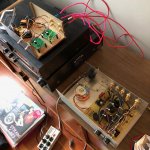
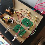
Got my boards back in January, and finally had a chance to finish wiring everything up today.
I went with a full dual mono setup because it seemed easier and fit the parts I had on hand. But... worked the first try. Very nice. Yes the L and R outputs are backwards. Easy enough to fix. In one of the photos you can see my old BOZ as well.
Think I'll fix the outputs, add a power switch, and button up my lovely new Bride.
Attachments
FYI some good input attenuation ideas back here if you have high input and too much gain:
https://www.diyaudio.com/forums/pass-labs/103050-jfet-boz-128.html#post3831402
https://www.diyaudio.com/forums/pass-labs/103050-jfet-boz-128.html#post3831402
I saw Nelson Pass' jfetBOZ idea and decided to play with it. Mostly because my old preamp just lost the left channel. What? It's as good an excuse as any, right?
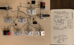
I looked at the circuit and all the variations of it (with other jfets, with and without feedback, etc...) and started laying it out. I tried to get pots for all the resistors that had different values in different circuits, so that I could tweak and see what happened. I ordered parts, cut up some aluminum angle iron, screwed it all down, and soldered it together.
It was build on a plywood chunk with pots everywhere. The only fixed values were the 1M and the 475 resistors. See the picture for details. A sharp eye will detect the miswire of the 1M and the missing ground on the input pot. Both have been fixed. Power goes in on the upper right, and the connections at the lower left read across a precision 1 ohm resistor to read Id directly in mV. The switch at the top cuts power to the whole board, and the switch just below middle enables or disables the feedback resistor (Rfb). The small bit straight across the top? Idss measurement circuit.
The first thing I did was check the Idss of all the devices (two matched sets of 4 and 20 random ones, from the usual sources). With that sorted (figuratively and literally), it was time to get going.
I started with the single worst device I had (Idss=10.7) figuring if I could get that to work, the low 7 and 6.5 values should be much easier. However, I wasn't getting the results I expected. H2 and H3 in the 30dB down range. Yuck! and the current kept climbing, slowly, but getting a bit high for my liking. Time to figure out what was wrong...
I busted out the old school books (I'm a EE, but I did digital and then went into software, so my advantage over the average hobbyist is just about nill) and dusted off my brain and went back to DC analysis of the circuit. I wasn't getting those values, so what could be wrong? Short power, open capacitors and... duh! Yep, the input cap I added to the design was on the wrong side of the 1M resistor and my gate was floating, slowly filling the input cap and increasing the Id flow...
A quick fix-up with the soldering iron and some checking of math and I tried it out. The predicted DC values for a Idss of 10.7 (a lone singleton in the set I got and by far the worst) checked out just fine. I tried one of a matched set (Idss of 6.5) and got what the math said, within a fraction (different vendor, different Vp, enough to alter Id a little, which ripples through the circuit).
Building Papa's version of the circuit with 24v supply (what I have) and the Idss=10.7 device left an resulted in 6.6v available across Vds. With the 6.5, it was nearly twice, at 12.6v available across the output (Vds). And both measured out correctly (mA and Vds).
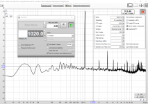
Ok, DC is fine, but how did it work with a signal? I used a Focusrite Solo (3rd gen) and REW to find out. Generating a 0.5Vpp 1khz sine wave at -3db (nearly full volume) into the input and with the volume knob all the way up, it had gain of about 22x, but the harmonics were bad (H2 -35, H3 -35), mostly because it was out of headroom. It was probably clipping a little bit, and the harmonics reflect that.
Starting with the box-stock circuit from Papa, the output voltage out was way beyond what I was looking for (and with lots of harmonics due to running at 24v instead of the recommended 35v), so I engaged the feedback circuit (switch to engage and disengage). With the gain down to 5x (0.5V in 2.5V out), I re-scaled the feedback loop and tried again. A little tweaking of Rd helped drop the H2 & H3 well down, and tweaking Rl helped knock H2 waaaaaayy down. How far? H2=-90dB, H3=-70dB, H4=-83dB. I cycled power a few times and got the same results. And then got a single odd response - H2=-95, H3=-85, but H4 jumped to -70dB. No idea what happened or why it did that, but the subsequent power cycles got the expected results..
The values for this run are as follows (as measured by a cheap DVM):
Rd = 2.5k
Rs = 10 ohms
Rl = 5.4k (max value of the pot)
Rfb = 16.5k
Rstop = 2.2k
Idss = 10.7mA
Id = 7.8mA
Harmonics: H2=-90dB, H3=-70dB (except one oddball on one power cycle)
Noise floor was about 100dB down (ignoring the power line noise - look at all those antennas) and the harmonic spikes.
With power removed (but the signal still going), the signal power dropped from 70.3dB to 6.3dB, the noise floor dropped from -30 to -50, although the harmonics were bad (H2=-16, H3=-30). What? I wanted to see what it looked like as a passive pre-amp. I hear they are all the rage in some circles.
Next couple of steps:
- trying a few different Rs values to see if I can get a better looking set of harmonics
- trying out the better devices (4x 6.4, 4x 6.5 and 4 in the 6.9-7.1 range) and see how the harmonics look with them in the circuit instead.
The only real measure of an audio circuit is listening. Unfortunately, it was a test tone, so it sounded like... a test tone.
- So, what do you think of the results? (see charts below)
- Was there anything I should have included that would help you analyze what is going on and help me improve the circuit?
- I presume the better devices will have improved (lower) harmonics due to more headroom, etc...
- I may put the scope in DC mode to make sure the input signal is centered in the envelope (Vds). I presume that will help with the distortion harmonics as well...
- Why do I want variable gain? I hate having to ride the volume knob as I switch sources, so I want to gain-stage at the pre-amp.
- The caps I'm using are junk I had in the drawer. For a high-quality pre-amp, what are some of the better go-to brands? I see so many names and so many recommendations across the site, I they have all blurred together.
So many questions. Hopefully some of the old-hands will have some ideas for me, and I'm happy to share what I've done and help however I can for the rest of you.
I looked at the circuit and all the variations of it (with other jfets, with and without feedback, etc...) and started laying it out. I tried to get pots for all the resistors that had different values in different circuits, so that I could tweak and see what happened. I ordered parts, cut up some aluminum angle iron, screwed it all down, and soldered it together.
It was build on a plywood chunk with pots everywhere. The only fixed values were the 1M and the 475 resistors. See the picture for details. A sharp eye will detect the miswire of the 1M and the missing ground on the input pot. Both have been fixed. Power goes in on the upper right, and the connections at the lower left read across a precision 1 ohm resistor to read Id directly in mV. The switch at the top cuts power to the whole board, and the switch just below middle enables or disables the feedback resistor (Rfb). The small bit straight across the top? Idss measurement circuit.
The first thing I did was check the Idss of all the devices (two matched sets of 4 and 20 random ones, from the usual sources). With that sorted (figuratively and literally), it was time to get going.
I started with the single worst device I had (Idss=10.7) figuring if I could get that to work, the low 7 and 6.5 values should be much easier. However, I wasn't getting the results I expected. H2 and H3 in the 30dB down range. Yuck! and the current kept climbing, slowly, but getting a bit high for my liking. Time to figure out what was wrong...
I busted out the old school books (I'm a EE, but I did digital and then went into software, so my advantage over the average hobbyist is just about nill) and dusted off my brain and went back to DC analysis of the circuit. I wasn't getting those values, so what could be wrong? Short power, open capacitors and... duh! Yep, the input cap I added to the design was on the wrong side of the 1M resistor and my gate was floating, slowly filling the input cap and increasing the Id flow...
A quick fix-up with the soldering iron and some checking of math and I tried it out. The predicted DC values for a Idss of 10.7 (a lone singleton in the set I got and by far the worst) checked out just fine. I tried one of a matched set (Idss of 6.5) and got what the math said, within a fraction (different vendor, different Vp, enough to alter Id a little, which ripples through the circuit).
Building Papa's version of the circuit with 24v supply (what I have) and the Idss=10.7 device left an resulted in 6.6v available across Vds. With the 6.5, it was nearly twice, at 12.6v available across the output (Vds). And both measured out correctly (mA and Vds).
Ok, DC is fine, but how did it work with a signal? I used a Focusrite Solo (3rd gen) and REW to find out. Generating a 0.5Vpp 1khz sine wave at -3db (nearly full volume) into the input and with the volume knob all the way up, it had gain of about 22x, but the harmonics were bad (H2 -35, H3 -35), mostly because it was out of headroom. It was probably clipping a little bit, and the harmonics reflect that.
Starting with the box-stock circuit from Papa, the output voltage out was way beyond what I was looking for (and with lots of harmonics due to running at 24v instead of the recommended 35v), so I engaged the feedback circuit (switch to engage and disengage). With the gain down to 5x (0.5V in 2.5V out), I re-scaled the feedback loop and tried again. A little tweaking of Rd helped drop the H2 & H3 well down, and tweaking Rl helped knock H2 waaaaaayy down. How far? H2=-90dB, H3=-70dB, H4=-83dB. I cycled power a few times and got the same results. And then got a single odd response - H2=-95, H3=-85, but H4 jumped to -70dB. No idea what happened or why it did that, but the subsequent power cycles got the expected results..
The values for this run are as follows (as measured by a cheap DVM):
Rd = 2.5k
Rs = 10 ohms
Rl = 5.4k (max value of the pot)
Rfb = 16.5k
Rstop = 2.2k
Idss = 10.7mA
Id = 7.8mA
Harmonics: H2=-90dB, H3=-70dB (except one oddball on one power cycle)
Noise floor was about 100dB down (ignoring the power line noise - look at all those antennas) and the harmonic spikes.
With power removed (but the signal still going), the signal power dropped from 70.3dB to 6.3dB, the noise floor dropped from -30 to -50, although the harmonics were bad (H2=-16, H3=-30). What? I wanted to see what it looked like as a passive pre-amp. I hear they are all the rage in some circles.
Next couple of steps:
- trying a few different Rs values to see if I can get a better looking set of harmonics
- trying out the better devices (4x 6.4, 4x 6.5 and 4 in the 6.9-7.1 range) and see how the harmonics look with them in the circuit instead.
The only real measure of an audio circuit is listening. Unfortunately, it was a test tone, so it sounded like... a test tone.
- So, what do you think of the results? (see charts below)
- Was there anything I should have included that would help you analyze what is going on and help me improve the circuit?
- I presume the better devices will have improved (lower) harmonics due to more headroom, etc...
- I may put the scope in DC mode to make sure the input signal is centered in the envelope (Vds). I presume that will help with the distortion harmonics as well...
- Why do I want variable gain? I hate having to ride the volume knob as I switch sources, so I want to gain-stage at the pre-amp.
- The caps I'm using are junk I had in the drawer. For a high-quality pre-amp, what are some of the better go-to brands? I see so many names and so many recommendations across the site, I they have all blurred together.
So many questions. Hopefully some of the old-hands will have some ideas for me, and I'm happy to share what I've done and help however I can for the rest of you.
Attachments

Have you tried the power supply in the 15v to 20v range?
While my bench power supply runs up to 32v, I've been focusing on 24v for the sole purpose of using an existing 24v power supply.
Also remember the circuit, as proposed by Papa, was running from a 35v power supply... For a reason - it gets Vds up to near the max of the part, so you are using absolutely every bit of power it can harness. Keeping the signal well centered and well below the max keeps it as linear as possible, so I'm already hurting my THD just by chopping the voltage by about a third...
*** What would you expect to see with a lower power supply range? ***
My understanding is the reduction in voltage will not change the voltage drop over Rd much, so it comes mostly out of the Vds. Presently, I'm losing about 17v in Rd, so if I drop from 24v to 20v, my Vds drops from just under 7v to just under 3v. Dropping to 15 would (I expect) cut the jfet out of saturation mode entirely, resulting in very ugly transfer across the load line... Am I missing something?
---
As an aside, my one and only jfet project in school ended in a bang. Well, not so much a bang as a pop. And then a puff of blue smoke (yes, for real, blue smoke). And the most gawd-awful nasty smell ever. So, I'm not exactly experienced in jfet circuits in specific, nor in analog circuits in general...
---
As another aside, my High School Senior project was to design a 3 digit 4-banger calculator at the logic-gate level (adder/multiplier functionality, decimal-to-bcd decoder, keypad decoder, the whole thing), in pencil, on velum. I'm digital to the bone!
---
Last edited:
Live has been keeping me busy, but here are some of my observations with the jfetBOZ circuit, as proposed by Papa (with an optional feedback resistor)
--- varying the Rs --- with feedback going
using the Idss=7.3 device, to get a better feel for how it will work when using the matched parts...
what trends are visible?
-lower Idss likes higher voltages
-lower Idss likes larger Rd values, lower Rs values
-larger Rd values work best with high Rl values
-larger Rs values like larger Rd values
--- varying the Rs --- this time, without feedback...
what trends are visible?
-more voltage to keep from clipping
-larger Rl & Rd will allow for better testing/tuning
I have a higher voltage power supply on order, along with larger Rl and Rd pots (and a smaller pot for Rs).
Perhaps next weekend I'll have an update with more useful data and observations...
--- varying the Rs --- with feedback going
using the Idss=7.3 device, to get a better feel for how it will work when using the matched parts...
Code:
 Rs  Vdd   H2   H3   H4   H5   THD    T+N    Id  Vds   Rd     Rl
 1.0  24  -80  -70  -82  -86  0.036  0.053  6.8  4.4  2.87k  5.41k*  maxed
      32  -95  -71  -83  -88  0.028  0.048  6.9  5.3  3.89k  5.41k*
 2.0  32  -87  -71  -82  -87  0.028  0.049  6.8  5.2  3.99k  5.41k*
      24  -92  -70  -83  -86  0.033  0.052  6.7  4.5  2.93k  5.12k  NOT maxed
 4.9  24  -75  -70  -82  -85  0.039  0.056  6.2  4.7  3.12k  5.41k* couldn't move H2
      32  -95  -71  -83  -86  0.030  0.050  6.2  5.0  4.34k  5.41k*
 7.1  32  -93  -70  -82  -85  0.035  0.054  5.8  4.8  4.66k  5.00k
      24  -90  -68  -82  -85  0.038  0.056  5.8  4.1  3.44k  4.37k
10.1  24  -92  -70  -82  -85  0.033  0.054  4.3  6.5  4.34k
      32  -95  -70  -82  -85  0.030  0.053  5.5       5.02k
14.3  32  -68  -72  -82  -85  0.045  0.060  5.0  5.3  5.31k*  5.41k*  BOTH are maxed
      24  -90  -68  -82  -85  0.039  0.055  4.9  3.8  4.10k  4.68k
25.8  24  yuck - nasty numbers
what trends are visible?
-lower Idss likes higher voltages
-lower Idss likes larger Rd values, lower Rs values
-larger Rd values work best with high Rl values
-larger Rs values like larger Rd values
--- varying the Rs --- this time, without feedback...
Code:
7.3 device
 Rs  Vdd   H2   H3   H4   H5   THD    T+N    Id   Vds   Rd     Rl     Idss  gain
 9.0  32  -60  -60  -75  -90  0.14   0.17    5.7  5.7  4.65k   5.41k*  7.3  18.0x
      24  -65  -60  -75  -90  0.11   0.14    4.7  7.1  5.23k   5.41k*  6.5  17.5x
15.6  yuck - nasty numbers
25.8 crap - even worse - 6%THD, 6.5v out on .5v in (peak to peak)
what trends are visible?
-more voltage to keep from clipping
-larger Rl & Rd will allow for better testing/tuning
I have a higher voltage power supply on order, along with larger Rl and Rd pots (and a smaller pot for Rs).
Perhaps next weekend I'll have an update with more useful data and observations...
Ok, now I feel dumb. In my desperation, I actually read the spec sheet and noticed that anything much over 0.2Vpp is going to distort... and I'm shoving in about 0.5Vpp...
Time to start over, with a more reasonable input voltage. Going to need a voltage divider pot at the front, to be able to drop the voltage small enough to not cream the little jfet. One must remember that the original point of this device was to amplify phono stages.
It all is becoming clearer... 😱
Time to start over, with a more reasonable input voltage. Going to need a voltage divider pot at the front, to be able to drop the voltage small enough to not cream the little jfet. One must remember that the original point of this device was to amplify phono stages.
It all is becoming clearer... 😱
- Home
- Amplifiers
- Pass Labs
- Jfet BOZ