Kanwar,
I`ve found this after one-hour search:
http://www.essex.ac.uk/dces/research/audio_lab/malcolmspubdocs/J10 Enhanced cascode.pdf
I`ve found this after one-hour search:
http://www.essex.ac.uk/dces/research/audio_lab/malcolmspubdocs/J10 Enhanced cascode.pdf
Jacco,
I strongly suspect that the MPS-U team, BD529 and its big brother BD419 (current amplifiers) were manufactured by Motorola under some form of agreement with the Japanese.
I strongly suspect that the MPS-U team, BD529 and its big brother BD419 (current amplifiers) were manufactured by Motorola under some form of agreement with the Japanese.
Kanwar,
there are some papers preaching a common collector stage between the transconductance and the transimpedance amplifier, but it has a poor theoretical bases (in my exceedingly humble view).
Do you mean like in a "constant power" differential configuration?
BTW, there are many of Dr Hawksfords electronic publications here. Happy reading.🙂
Questions- it is true the emitter resistors on the diff pair gives wider bandwidth, less gain, and are more linear, right? On the other hand this bandwidth and linearity comes at an increase in delay time through that stage, correct? Same for a common collector in front of the VAS, more delay, right?
In my best estimation linearity has not been much trouble using "modern" parts while delay is always a problem causing the loop to be unstable (lack of phase margin or whatever).
What is anyone's thoughts on delay as reduced delay is the design goal here? Time through the amplifier seems seldom discussed.
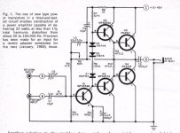
The attached amp still calls for that best VAS transistor the subject of the thread but really has a lot less delay and less parts. What about thisn for AC signals? Not to difficult to achieve .1%THD with modern parts. Thoughts?
Note, would not use that exact output and driver stage.
In my best estimation linearity has not been much trouble using "modern" parts while delay is always a problem causing the loop to be unstable (lack of phase margin or whatever).
What is anyone's thoughts on delay as reduced delay is the design goal here? Time through the amplifier seems seldom discussed.
The attached amp still calls for that best VAS transistor the subject of the thread but really has a lot less delay and less parts. What about thisn for AC signals? Not to difficult to achieve .1%THD with modern parts. Thoughts?
Note, would not use that exact output and driver stage.
Attachments
Kanwar,
I`ve found this after one-hour search:
http://www.essex.ac.uk/dces/research/audio_lab/malcolmspubdocs/J10 Enhanced cascode.pdf
Thanxz for the link, i have seen it already but i can't see anything discussed on rush-cascode, rather all the literature is focused on normal versions of cascode and some enhancements.🙂
sumaudioguy,
That`s correct.Questions- it is true the emitter resistors on the diff pair gives wider bandwidth, less gain, and are more linear, right?
That`s not correct. The propagation delay is caused by slow electron mobility, two inbuilt P-N junctions and bipolarity. Basically, this is also the reason for the more impure distortion pattern bipolar transistors exhibit. You cannot get around the time delay, its effect becomes rather deleterious with an applied global feedback.On the other hand this bandwidth and linearity comes at an increase in delay time through that stage, correct?
CBS240
I mean a common collector stage before the VAS in any configuration. The theory has been utilized in many (British) designs.
I mean a common collector stage before the VAS in any configuration. The theory has been utilized in many (British) designs.
Kanwar,
there are some papers preaching a common collector stage between the transconductance and the transimpedance amplifier, but it has a poor theoretical bases (in my exceedingly humble view).
In my conceptual schematic, i no where used any common collector stage to buffer VAS.
Last edited:
Kanwar,
the upper and lower transistors in post #86 are by definition common-collector amplifiers.
the upper and lower transistors in post #86 are by definition common-collector amplifiers.
sumaudioguy,
That`s not correct. The propagation delay is caused by slow electron mobility, two inbuilt P-N junctions and bipolarity. Basically, this is also the reason for the more impure distortion pattern bipolar transistors exhibit. You cannot get around the time delay, its effect becomes rather deleterious with an applied global feedback.
Not correct for the circuit? I agree and understand the intrinsic delay of the device but with the emitter degradation resistors causing increase in voltage swing on a diff pair which increases the effects of any capacitance in the diff pair thereby slowing (increasing delay) of that diff pair output to the next stage. What is wrong with this thought? My measurement at the input to the VAS transistor say this is exactly what happens, both current and voltage are delayed with increases in the diff pair emitter resistors. Kindly explain?
Thanks-
Kanwar,
the upper and lower transistors in post #86 are by definition common-collector amplifiers.
That is CC-CB stage, not the usual CC stage feeding CE in buffered VAS like in D.Self's amplifiers. Even in normal Cascode we have CE-CB. The stage which i use is very different from other stages i just mentioned along with its different set of associated features.
Kanwar,
it does no good. I think the voltage buffer idea stems from diffuse theories by Hawksford and D. Self talking about slope distortion and base currents that have no relevance.
it does no good. I think the voltage buffer idea stems from diffuse theories by Hawksford and D. Self talking about slope distortion and base currents that have no relevance.
The main properties of the common base amplifier:
¤ low input impedance (approaches the ideal, gives high noise immunity)
¤ low feedback factor giving
¤ high isolation between input and output
¤ high stability and
¤ wide bandwidth due to the absence of Miller effect and small base-emitter input capacitance
¤ wide dynamic range
¤ high input overload capability
¤ precisely controlled voltage gain
¤ current gain just below 1 (low power gain gives low distortion)
¤ the same amount of current flows through the input and output and in unbalanced mode through the signal source (gives low distortion)
¤ no phase reversal between input and output
Now, the output voltage varies exponentially with the input voltage, which means poor linearity, so the input signal has to be a current (just as it should be)
BJT is current controlled device😉
@WuYit,
CC-CB combo definitely has many advantages, in order to figure them out you need to think about them😉
@WuYit,
CC-CB combo definitely has many advantages, in order to figure them out you need to think about them😉
well that depends on how you look at it. Vbe & re can be related to conductance, thus voltage controled.
however when making a BJT circuit, I find it often helps to think of them as 'current' controled. It does require a specific amount of minority carriers to control the transistor.
however when making a BJT circuit, I find it often helps to think of them as 'current' controled. It does require a specific amount of minority carriers to control the transistor.

Once the BJT is "biased up" in class A operation or quiescent point the input is fairly current like. From "off" there is a lot of voltage potential required to make anything significant happen. A threshold of activation then another region of operation.
As a novel approach, I actually find it more useful to consider a BJT a thermal device. As carriers/holes move (translate position) there is an increase in temperature. Causing temperature increase in one part of the device (base emitter) results in an increase in temperature of the collector emitter. Am not trying to "sell" this idea to anyone. Just mentioning it. 🙂
As a novel approach, I actually find it more useful to consider a BJT a thermal device. As carriers/holes move (translate position) there is an increase in temperature. Causing temperature increase in one part of the device (base emitter) results in an increase in temperature of the collector emitter. Am not trying to "sell" this idea to anyone. Just mentioning it. 🙂
- Home
- Amplifiers
- Solid State
- It's 2010 and what's your fav VAS transistor?