Hello guys,
I modified a MosFET based 100w amplifier, I'd like to know if the resulting simulation is good enough for an actual build. Any thoughts?
Many Thanks!
I modified a MosFET based 100w amplifier, I'd like to know if the resulting simulation is good enough for an actual build. Any thoughts?
Many Thanks!
Attachments
Hi Abetir,
The front-end (IPS+VAS) is fine, but the output stage is a problem for two reasons:
1) No thermal feedback. Setting the bias with a simple trim pot is fine if you use the Lateral MOSFETs (like Hitachi's K1058/J162), but with the HexFETs you use, the spreader, placed on a heatsink with the output devices, is a must. Otherwise, a thermal runaway is going to happen.
2) HexFETs have got a high, non-linear input capacitance, so the driver stage is required if you want to have a good result in terms of distortion. Again, Laterals are ok to connect directly to VAS - their input capacitance is lower and much more linear.
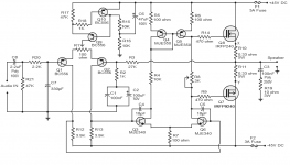
Here is an example of what a good HexFET output stage looks like:
HexFET OPS
This one has got 5 pairs of IRFPs, but even with one pair the principle is the same. The spreader and the drivers.
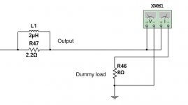
Attached is the right way of connecting the watt-meter.
Cheers,
Valery
P.S. You can also see this thread and the way it came to the working circuit in the end (with regards to the bias spreader):
http://www.diyaudio.com/forums/solid-state/286540-ab-amplifier-oscillating-seeking-critique.html
The front-end (IPS+VAS) is fine, but the output stage is a problem for two reasons:
1) No thermal feedback. Setting the bias with a simple trim pot is fine if you use the Lateral MOSFETs (like Hitachi's K1058/J162), but with the HexFETs you use, the spreader, placed on a heatsink with the output devices, is a must. Otherwise, a thermal runaway is going to happen.
2) HexFETs have got a high, non-linear input capacitance, so the driver stage is required if you want to have a good result in terms of distortion. Again, Laterals are ok to connect directly to VAS - their input capacitance is lower and much more linear.
Here is an example of what a good HexFET output stage looks like:
HexFET OPS
This one has got 5 pairs of IRFPs, but even with one pair the principle is the same. The spreader and the drivers.
Attached is the right way of connecting the watt-meter.
Cheers,
Valery
P.S. You can also see this thread and the way it came to the working circuit in the end (with regards to the bias spreader):
http://www.diyaudio.com/forums/solid-state/286540-ab-amplifier-oscillating-seeking-critique.html
Attachments
be careful; i would find it hard to believe that output stage has stable biasing.
mlloyd1
You were just a bit faster 🙂 But shorter 😛
At the output resistor it measures +-15.42v (VP_17/18 in the table) is this OK?
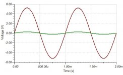
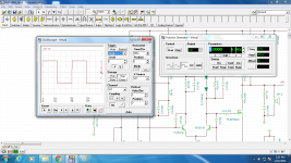
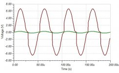
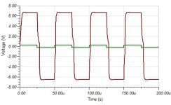
The still image of the squarewave looks nice but in the interactive simulation a very short overshooting occurs at the high freq.
Thank you guys for the feedback.
@Valery,
I would like to stick with the HexFet, Laterals comes very expensive here in my place. 🙁 Thank you for the link.
Cheers! 🙂
The still image of the squarewave looks nice but in the interactive simulation a very short overshooting occurs at the high freq.
Thank you guys for the feedback.
@Valery,
I would like to stick with the HexFet, Laterals comes very expensive here in my place. 🙁 Thank you for the link.
Cheers! 🙂
Attachments
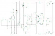
Audio Gurus and all,
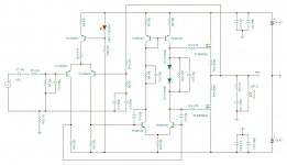
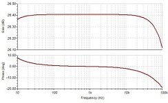
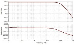
Hello again, I made a new revision of my first schematic I have added BJT drivers and reconfigure the VAS CCS in order to feed more current to bias VBE but I'm kind of stuck here...would any of you be so kind in helping me straighten out those curves in the graph? (attached below) As I am a hobbyist perhaps my approach is leading me into circles and missing the right spot to where the error/fault lies.
Data taken from simulation software follows,
Amplitude 250mv
Freq. 20Khz
Harmonic Distortion = 9.5704%
DC offset 3.3mv
Output resistor IRFP240 = 3.64mv
IRFP9240 = 3.53mv
Gate voltage IRFP240 = 3.77v
IRFP9240 = 2.46v
Bias trimpot set at 50%
What I have done so far,
added small resistor at the bases of drivers, no effect
added small value cap between base/collector also, no effect
added small value lead cap connected to base of driver, THD rises
100pf at C12 minimal reduction on THD figure.
This is my first attempt working with MosFet based amplifier and I wanted to do it right the first time. Pointers, advise, recommendations is very much welcome and I will do my research.
Kind Regards!
Albert
@Valery, I did adapt your bias spreader scheme but it looks though that it works the same as with my schematic.(or my implementation could be wrong)
Attachments

T7 is a n-channel source follower.
T8 is a p-channel with source to negative rail - something wrong in the schematic, I think it should be flipped vertically and the bias increased
T8 is a p-channel with source to negative rail - something wrong in the schematic, I think it should be flipped vertically and the bias increased
T8 is a p-channel with source to negative rail - something wrong in the schematic, I think it should be flipped vertically and the bias increased
There is nothing wrong. Look again...
I get the feeling that the sch in posts 1 & 2 are showing a bad conversion from Lateral mosFET to Vertical mosFET.
Beware, omitting temperature compensation. Vertical mosFETs may blow up.
Post7:
the diodes and Zeners on the output gates have been swapped.
Beware, omitting temperature compensation. Vertical mosFETs may blow up.
Post7:
the diodes and Zeners on the output gates have been swapped.
Audio Gurus and all,
Hello again, I made a new revision of my first schematic I have added BJT drivers and reconfigure the VAS CCS in order to feed more current to bias VBE but I'm kind of stuck here...would any of you be so kind in helping me straighten out those curves in the graph? (attached below) As I am a hobbyist perhaps my approach is leading me into circles and missing the right spot to where the error/fault lies.
Data taken from simulation software follows,
Amplitude 250mv
Freq. 20Khz
Harmonic Distortion = 9.5704%
DC offset 3.3mv
Output resistor IRFP240 = 3.64mv
IRFP9240 = 3.53mv
Gate voltage IRFP240 = 3.77v
IRFP9240 = 2.46v
Bias trimpot set at 50%
What I have done so far,
added small resistor at the bases of drivers, no effect
added small value cap between base/collector also, no effect
added small value lead cap connected to base of driver, THD rises
100pf at C12 minimal reduction on THD figure.
This is my first attempt working with MosFet based amplifier and I wanted to do it right the first time. Pointers, advise, recommendations is very much welcome and I will do my research.
Kind Regards!
Albert
@Valery, I did adapt your bias spreader scheme but it looks though that it works the same as with my schematic.(or my implementation could be wrong)
Hi Albert,
OK, a few quick comments.
Quiescent current of the output transistors is way too low. Voltage drop over R15, R16 has to be around 22mV each. It's better to measure over both of them - right between the sources - in this case it would be 44mV. Adjust it with P1.
T3, T4 arrangement (cascode) is not necessary here - it dis-balances the current mirror. Remove T4, R23, R29.
If you specify the quiescent current at each stage - it will be easier to analyze - I mean, collectors of T1, T2, T5, T6, T11, T7.
Compensation is a separate story - let's make it working in general first.
Cheers,
Valery
Last edited:
Hi guys,
Here's a revised schematic and the measurement,
corrected zener/1N4148 at the output gates
removed T4, R23, R29
T1/R4 = 865.04uA
T2/R5 = 860.7uA
T3/R18 = 421.34uA
T5/R24 = 2.01ma
T6/R21 = -397.84uA
T10 VBE = 4.22v
T11 driver = 41.29v
T12 driver = -41.29v
T7/R15 = 277.49uA
T8/R16 = 47.25uA
@Valery ,
I could not find the ma measurement for the output Fets but measuring the fuses I get,
+rail fuse = -324.48uA (yes with the minus sign)
-rail fuse = +319.41uA
Harmonic distortion = 8.263%
DC offset = 1.9mv
P1 bias adjustment does not seem to be working 0-90% set, shows the same measurement on the outputs.
LED2 bias goes off.
Many Thanks!
Albert
Attachments
That circuit is based on an old 1980's Hitachi lateral mosfet application note.
It has had current mirror and current source added to it.
The biasing is terrible, it really needs a Vbe multiplier.
As it is you will get crossover distortion quite badly.
It has had current mirror and current source added to it.
The biasing is terrible, it really needs a Vbe multiplier.
As it is you will get crossover distortion quite badly.
The original circuit...
The design is described here, not so sure if these guys are the original designer (the circuit seemed to have evolved into a few variants). It is surprising though that it has a bandwith of 4Hz-4KHz..
Attachments
The original circuit was used by Maplin in the 1980's in their mosfet amplifier.
It was designed to be a cheap as possible.
I updated the design myself last year for ALF laterals.
I also added extra RC decoupling on the front end to reduce hum.
I added front end constant current source and a two transistor current mirror.
It was designed to be a cheap as possible.
I updated the design myself last year for ALF laterals.
I also added extra RC decoupling on the front end to reduce hum.
I added front end constant current source and a two transistor current mirror.
Hi nigelwright,
Can I have a look at this circuit of yours?..was the Maplin design contains driver stage? I've been searching for days to find an IRFP240/9240 mosfet based amplifier that has a driver stage, but it seemed those circuit that had driver stage are symmetrical by design if not overly complex 🙂
It is quite hard to run an overly complex circuit in simulation wares, it'll force you to edit the analysis parameters set by default in the software otherwise you will be getting a lot of convergence errors 🙁
What I was looking for is a working driver stage that can be fitted to work with my simple circuit.
Cheers!
Albert
Original circuit used by Maplin and taken from Hitachi mosfet application note.
An externally hosted image should be here but it was not working when we last tested it.
Post #1 has an error in the P-channel, showing source to negative supply.There is nothing wrong. Look again...
Post #2 is electrically correct, but the symbol is misleading as the convention is for the gate connection to be next to the source
Post #7 onwards is correct
Original circuit used by Maplin and taken from Hitachi mosfet application note.
An externally hosted image should be here but it was not working when we last tested it.
This circuit looks popular all over the net, and a lot of variants too, some uses LatFet while others used HexFet with the addition of gate diodes. I've been reading a few comments from builders and a few problem exists here and there...🙁
- Home
- Amplifiers
- Solid State
- IRFP240/9240 Amplifier (simulated on TINA)