Another idea i have is to increase the bias current only near zero volts area where is the distortion. maybe this is even better
you will thank me for this idea.
you will thank me for this idea.
Last edited:
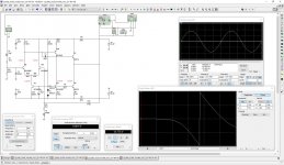
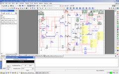
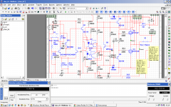
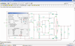
Front-end DC analysis and basic performance indicators
OK, as promised. Did not even touch stability yet - too many issues of the lower level of complexity.
Let's put the output stage aside for now. First of all, we need a well-performing voltage gain stage.
Your operating points combination is confusing. Guessing? Random choice?
Very low quiescent currents for LTP and VAS and then... BD139 will feel bad at 56.6mA (more than 1.3W of dissipation). For what reason?
Next post - some ways to improve it.
Attachments

Last edited:
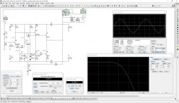
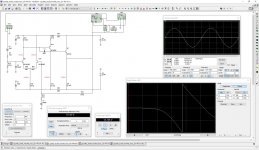
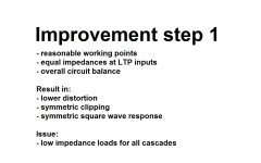
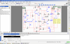
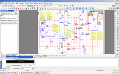
Some simple ways to improve the performance
OK, the last attempt to convince you reading some books.
Trying to keep it as simple as possible. Keeping your choice of active devices and overall topology.
1-st step - just making operating points reasonable and matching the impedances.
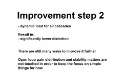
2-nd step - adding dynamic loads.
There are many ways to make it even better. There are many people here, who can do it better than me. There is a lot of good material on amplifiers design in general and "blameless" topology - the one you're using here - in particular.
Saying "I don't care - it sounds good" - your choice. But I'm afraid it will sound good only for you in this case 😉
OK, the last attempt to convince you reading some books.
Trying to keep it as simple as possible. Keeping your choice of active devices and overall topology.
1-st step - just making operating points reasonable and matching the impedances.
2-nd step - adding dynamic loads.
There are many ways to make it even better. There are many people here, who can do it better than me. There is a lot of good material on amplifiers design in general and "blameless" topology - the one you're using here - in particular.
Saying "I don't care - it sounds good" - your choice. But I'm afraid it will sound good only for you in this case 😉
Attachments
-
 21-MosFET-01.JPG282.1 KB · Views: 99
 -
 21-MosFET-02.JPG280.6 KB · Views: 87
 -
 21-MosFET-03.JPG282.5 KB · Views: 84
 -
 21-MosFET-04.JPG280.1 KB · Views: 90
 -
 21-00-Title-01.JPG140.9 KB · Views: 93
 -
 11-MosFET-04.JPG274.1 KB · Views: 78
 -
 11-MosFET-03.JPG276.1 KB · Views: 80
 -
 11-MosFET-02.JPG274.5 KB · Views: 100
 -
 11-MosFET-01.JPG276.2 KB · Views: 99
 -
 11-00-Title-01.JPG143.5 KB · Views: 94
These values were for close to zero offset. When i made both ltp currents equals it resulted in a very big offset.Your operating points combination is confusing. Guessing? Random choice?
BD139 will feel bad at 56.6mA (more than 1.3W of dissipation). For what reason?
Im heatsinking it. For more IPS output current.
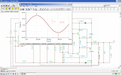
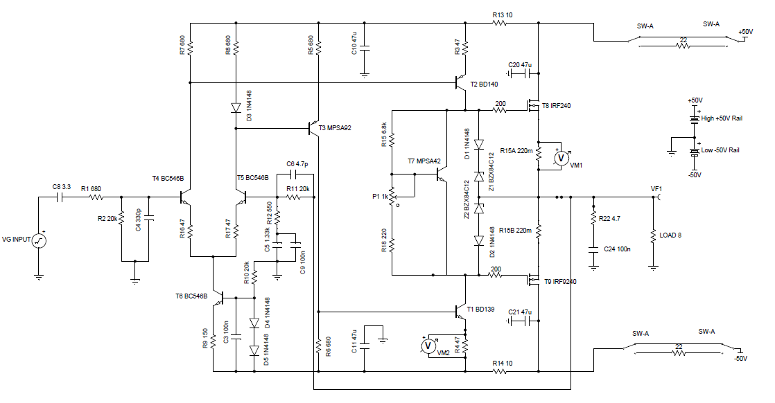
vzaichenko, this is my updated version,
I calculated that 27mA for the ips bd139 will be good without heatsinking.
This means 1.1k 0.5W R1 resistor.(2x2.2k or 2x2.4k in parallel)
*In sch is 3.3k because i calculated it after that.
What is the Pc of BD139 with a very small heatsink>? Minimum size one. I have one very small and want to use it squizing max current from the IPS. I know i am not needing but want to use the heatsink 😀 (My goal is 2W Pc from 1.25 -> 2W)(maybe this is possible with the smallest one but what about 4W ? )
R8 is 22.8k in simulation only, for fine tuning (its22k)
I am confused about the optimal values of R18.(without volume pot)
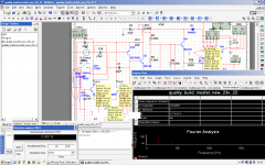
fft analys is @ 20khz.
i readt from here -> https://en.wikipedia.org/wiki/Line_level
that line level is 0.316V for consumer audio.
And i tuned it for it. Its perfect scaled.
This 1000000 times better than this im listening now. :OOO
I calculated that 27mA for the ips bd139 will be good without heatsinking.
This means 1.1k 0.5W R1 resistor.(2x2.2k or 2x2.4k in parallel)
*In sch is 3.3k because i calculated it after that.
What is the Pc of BD139 with a very small heatsink>? Minimum size one. I have one very small and want to use it squizing max current from the IPS. I know i am not needing but want to use the heatsink 😀 (My goal is 2W Pc from 1.25 -> 2W)(maybe this is possible with the smallest one but what about 4W ? )
R8 is 22.8k in simulation only, for fine tuning (its22k)
I am confused about the optimal values of R18.(without volume pot)
fft analys is @ 20khz.
i readt from here -> https://en.wikipedia.org/wiki/Line_level
that line level is 0.316V for consumer audio.
And i tuned it for it. Its perfect scaled.
This 1000000 times better than this im listening now. :OOO
Attachments

Last edited:
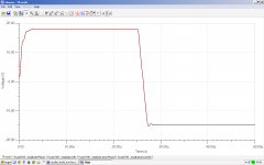
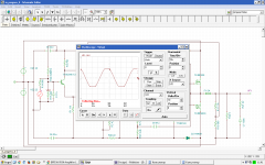
Im ready with my class Ai (improved) 😀
Im using optocoupler to hightening the bias (maximum @ zero volts input) 😀
Normally its 70-80mA. When input goes close to ground, it goes linearly to 760mA. This provides class A only when its needed, near crossover region.
Im not sure is it correct, i should bias this optoled and his katode must be to ground 😀
Attachments

up,
R8 is 22k
R1 is 2x2.2k 0.25W
for 23V, optimal bias current is 250mA,
im going to simulate it in TINA,
interesting ;p
R8 is 22k
R1 is 2x2.2k 0.25W
for 23V, optimal bias current is 250mA,
im going to simulate it in TINA,
interesting ;p
Attachments
Last edited:
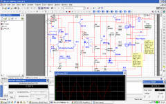
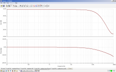
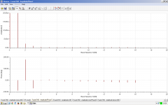
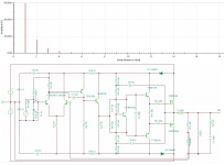
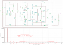
->->->TINA results:
THD@1khz->0.04% (better than Multisim)
THD@20khz->0.72% (worse than Multisim)
offset@DC->63mV
offset@AC->very big :O
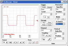
square->excellent 😀 😛
THD@1khz->0.04% (better than Multisim)
THD@20khz->0.72% (worse than Multisim)
offset@DC->63mV
offset@AC->very big :O
square->excellent 😀 😛
Attachments

Last edited:


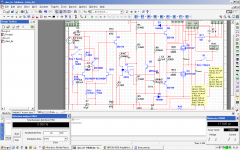
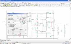
new tina results with this setup.
there is only 1 last thing to modify the ops a little bit.
i designed it for 2 to 4 Vth but it must be little higher (Vth+Vbias(256mA))
if im using mosfets with 4V thrs voltage i will be unable to set the 256 mA bias current. 🙄
P.S. i forgot to change R4 to 4.7k. i need to test again 🙁
P.S.2. This is my first time using the MEGAOHM resistance range 😀 (R24==7.5MEG)
P.S.3. Gives 0.1% THD @ 1khz and 0.7% @ 20khz.
Attachments

Last edited:
I am doing a mod to Apex's FX8 to use hex FETs and found that adding a 0.22R resistor at the supply/drain pins between the output seems to reduce distortion. Running at 150mA bias seems to be working right now. Try adding it to TINA sim and see how it works.
http://www.diyaudio.com/forums/solid-state/164093-100w-ultimate-fidelity-amplifier-725.html
http://www.diyaudio.com/forums/solid-state/164093-100w-ultimate-fidelity-amplifier-725.html
I am doing a mod to Apex's FX8 to use hex FETs and found that adding a 0.22R resistor at the supply/drain pins between the output seems to reduce distortion. Running at 150mA bias seems to be working right now. Try adding it to TINA sim and see how it works.
http://www.diyaudio.com/forums/solid-state/164093-100w-ultimate-fidelity-amplifier-725.html
Hi,
If I can add my 2 cents...
HexFETs (like IRFP240/9240) behave pretty bad when driven directly from VAS due to their high non-linear input capacitance. It order to achieve a good result, you need a EF driver stage. See a simple output stage here:
VHex initial schematic
On the other hand, Lateral FETs are ok to run directly from VAS:
VLatFET+ schematic and live measurements
Although, with the driver stage distortion will be even lower.
Cheers,
Valery
The simulations showed reasonably low distortion (-65dB H3) with the VAS driving the vertical MOSFET directly. Help me understand why another stage is needed as FET gates are voltage devices with no current draw - would not even a tiny TO93 transistor be able to drive it? How does another stage overcome the high non linear input capacitance?
The measured speaker harmonic distortion sign the hexFET was actually lower than the lateral FET version.
The measured speaker harmonic distortion sign the hexFET was actually lower than the lateral FET version.
Valery is right, you need to drive the high input capacitance (hexFET) from a low impedance node. The VAS stage has a high output collector output impedance, thats why you need an emitter follower.
Ok - I will give it a try. Interesting how the sim as is seems ok and it sounds good. I guess it can be even better.
I have strayed so far off from an FX8 I don't think it can legitimately even be called an FX8 mod if I do this. The topology and OPS is very different. Same input front end and CM but that is pretty basic from what I have seen.
I have strayed so far off from an FX8 I don't think it can legitimately even be called an FX8 mod if I do this. The topology and OPS is very different. Same input front end and CM but that is pretty basic from what I have seen.
The simulations showed reasonably low distortion (-65dB H3) with the VAS driving the vertical MOSFET directly. Help me understand why another stage is needed as FET gates are voltage devices with no current draw - would not even a tiny TO93 transistor be able to drive it? How does another stage overcome the high non linear input capacitance?
The measured speaker harmonic distortion sign the hexFET was actually lower than the lateral FET version.
They are high impedance but thats why because their impedance gets lower as freq goes high.(capacitance reactance) For example -> irf530 have 670pf input capacitance and with 20khz this forms 11.877k resistor to source ;p(much lower gate input impedance)
=> my R11 must be 5.9385k instead 330 => with 330 i can drive 5.9k/330 = 18 pairs of mosfets.
hey i can use tiny TO93 if im using one pair only.
search google "capacitance reactance calculator". this shows resistance of a capacitor @ a freq.
This is also why you need low value gate stoppers. iT seems that my 220r is high again. i must use 100 ones.
I am doing a mod to Apex's FX8 to use hex FETs and found that adding a 0.22R resistor at the supply/drain pins between the output seems to reduce distortion. Running at 150mA bias seems to be working right now. Try adding it to TINA sim and see how it works.
Exactly opposite. They result in worse distortion, see. I readjusted idle current with them because it gets lower.
Attachments
Last edited:
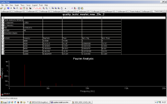
Vz, i made it with very good result. Harmonics are not visible 😀
THD == 0.022%
DC Offset == -84mV
P.S. Its better with R4=2k and R2=4.7k. Btw is 32mA good for BDs without heatsink ? This is 736mW Pd with 23V.
Next update is to change T6 and T7 with BCs546/556 and R11 with 5.6k for only 1 pair of mosfets, this is 2x80W amp, not powerfull beast.
P.S.2 There is 0nly 56.14uA difference in LTP collector currents.;p
Attachments
Last edited:
- Status
- Not open for further replies.
- Home
- Amplifiers
- Solid State
- IRF530/9530 Amplifier (simulated in Multisim and TINA)