It is possible that your power supply cannot deliver enough current.
Try connecting a 10R load resistor directly to the power supply and
see if the voltage collapses when sourcing 1.2ADC.
Try connecting a 10R load resistor directly to the power supply and
see if the voltage collapses when sourcing 1.2ADC.
It is possible that your power supply cannot deliver enough current
My power supply can can handle the current. I think my problems is when I check the driver high output it is measuring a peak to peak of 20v and not 12v. What could be this cause of this?
Last edited:
Several possibilities, unfortunately .. and sorry to say, but the most likely is a 'cockpit problem'. Measuring anything HI side is tricky. Unless you're using a high voltage differential probe, the additional capacitance to ground and the ringing that goes with long ground-return loops can produce all manner of spurious measurements.
Are you blowing HI side MOSFET's? Do you have some other reason for suspecting excessive Vcc? Earlier the problem was collapsing Vcc; has that gone away? While we're on the subject, the UF4007 is ALSO unsuitable as a bootstrap rectifier.
What are you using for a load for these tests? If inductive, you'll need to include something resistive in the circuit to dissipate some of the power.
Time to post a picture of your test setup? Maybe even an updated schematic?
Cheers
Can you post some waveforms? The upper gate will be at +24VDC wrt ground when
the upper device is on, because of the charge pump action.
the upper device is on, because of the charge pump action.
Last edited:
Sorry, that was a mistake. I measured the output of the Low side.Measuring anything HI side is tricky. Unless you're using a high voltage differential probe, the additional capacitance to ground and the ringing that goes with long ground-return loops can produce all manner of spurious measurements.
No, I checked the MOSFETs and they are fine. Also, Vcc is still collapsing but I was able to measure the output of the low side before it collapsed and I realise it was 20v. I though UF4007 are good for bootstrap. Should I use the 1N4148.Are you blowing HI side MOSFET's? Do you have some other reason for suspecting excessive Vcc? Earlier the problem was collapsing Vcc; has that gone away? While we're on the subject, the UF4007 is ALSO unsuitable as a bootstrap rectifier.
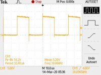
I am just testing the power stage (gate driver and MOSFETs) to make sure they are working accordingly. The image is the output of Pin 1 of the Ir2110 driver.
will the 1N4148 and an electrolytic 22uF be good for the bootstrap circuit. Should I forget the external deadtime and just send the inverse signals to H bridge because the IR2110 has an internal deadtime because I think the deadtime is affecting the driver. When I test the driver on its own without the bootstrap circuit, the peak to peak of the high and low side are 12v.
Attachments
Last edited:
You need a heavier duty diode for the charge pump, the UF4007 would be ok. A 22uF capacitor might work,
but increase the value to 100uF if the low switching frequency causes too much droop during the on period.
If the voltage droops too much, the device will not remain saturated, and will enter the linear region for a time
before it switches off.
but increase the value to 100uF if the low switching frequency causes too much droop during the on period.
If the voltage droops too much, the device will not remain saturated, and will enter the linear region for a time
before it switches off.
Last edited:
The 1N4148 would only suffice for testing at low MOSFET supply voltages, say 20 or 25V.
Sorry I forgot to answer your earlier question, 'Can half-bridge drive a sub-woof?' -- Yes.
But to avoid having a giant coupling cap for the output, the power supplies get a little tricky to keep straight. And if you choose bi-polar (supplies), then you have to devise a high-speed level shifter, which isn't usually much fun.
No reason to worry about the 1V droop in the 15usec On portion of the scope waveform in post #25. The test 'load' was probably resistive, eh? If that's why you fit the 22uF electrolytic for the bootstrap, it was misguided. The bootstrap capacitor has to charge fully in whatever the minimum Lo-side-On interval is. A 0,47 or 1uF ceramic is often fine, though at a switching frequency this low, maybe a little higher -- still looking for that application note for you.
The bootstrap rectifier needs to be fast, low-capacitance, have a very hard knee, and well-higher PIV than the maximum output swing.
By the way, the leading edge spikes on the waveform spell 'long 'scope probe ground lead'. MOSFET Gates hate those.
I'm gonna take a minute and go double check the IR2110 PDF on your deadtime question.
Regards
edit: Apologies to rayma -- gotta find that App Note, yet -- but in normal (non-test) operation, there's no DC load to cause droop.
Last edited:
OK, just finished reviewing the IR2110 specs and it doesn't have any provision to control deadtime. There's an ~25nsec shorter turn-off delay, than turn-on; but channel to channel matching eats up 10nsec of that, so best handle it explicitly. Handily, the LIN and HIN's are Schmitt trigger inputs -- perfect spot for the diode/RC edge delay. Just make sure you have close matching in the opposite-phase drive waveforms. XOR's are handy there - use one buffer, one inverter - but don't drive both inputs with the same signal. Methinks that might be the source of trouble in your CD4070 application earlier: All you get at the output are a smattering of very small spikes.😉
In general, even if driving two logic gate inputs provides the desired output, the extra capacitance slows things unnecessarily. Only do it if it solves a layout nightmare.
Cheers
In general, even if driving two logic gate inputs provides the desired output, the extra capacitance slows things unnecessarily. Only do it if it solves a layout nightmare.
Cheers
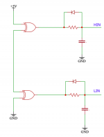
Do you mean the should put the diode/Rc delay before the inputs? Also, close matching? Do you mean that the both driver input should have the same waveforms.Handily, the LIN and HIN's are Schmitt trigger inputs -- perfect spot for the diode/RC edge delay. Just make sure you have close matching in the opposite-phase drive waveforms
Can you explain more.XOR's are handy there - use one buffer, one inverter - but don't drive both inputs with the same signal
I'm a tad bit confuse as to the circuit your are recommending. Should I go ahead with the diode/RC delay with the 7414 Schmitt trigger or use the XOR gate. If you provide a circuit, it would very much appreciated.
Last edited:
OK, yeah my explanations could be better .. I'll need some time this evening to work on it.
In the mean time, just noticed: The R15/R16 divider places the midpoint of the oscillator waveform at Vcc / 2. Maybe that's leftover from an earlier design, but pretty sure you'll want that centered around ground.
In the mean time, just noticed: The R15/R16 divider places the midpoint of the oscillator waveform at Vcc / 2. Maybe that's leftover from an earlier design, but pretty sure you'll want that centered around ground.
Will this deadtime circuit be sufficient?
Yes, I want it centred around the zero. So you think I should remove the negative supply and remove the diver I place an AC coupling at the output?In the mean time, just noticed: The R15/R16 divider places the midpoint of the oscillator waveform at Vcc / 2. Maybe that's leftover from an earlier design, but pretty sure you'll want that centered around ground.
Attachments
Last edited:
Yep -- that's strangely similar to what I spent twice-as-long cobbling up .. 😉
One gate inverts, one doesn't, delays approx equal. Not sure about which should be HIN and which LIN, though. *
And pretty sure the output HAS to be DC-coupled; but it will depend on your output filter and feedback network. *
Cheers
edit: These R/C values should give about 50 nsec of deadtime. Feel free to change them; at 30 kHz switching, there's plenty of room to experiment.
edit2: The J1 wiring will cause the ring channel to be subtracted from the tip channel.
One gate inverts, one doesn't, delays approx equal. Not sure about which should be HIN and which LIN, though. *
No, keep the negative supply. Remove the divider. Everything gets harder to keep straight if Signal-Ground is not Ground-Ground.So you think I should remove the negative supply ..
And pretty sure the output HAS to be DC-coupled; but it will depend on your output filter and feedback network. *
Cheers
edit: These R/C values should give about 50 nsec of deadtime. Feel free to change them; at 30 kHz switching, there's plenty of room to experiment.
edit2: The J1 wiring will cause the ring channel to be subtracted from the tip channel.
Attachments
Last edited:
Hi, thank you so much for your help. I will test your circuit and hopefully the o=low side output will be 12v.
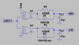
XOR, but either would work -- just swap the 2nd (non-LM311) inputs -- change the one connected to Vdd to ground, and the one to ground to Vdd.
Sorry about the funny-looking symbol. I don't know how to delete the extra ins/out in LT Spice.
Sorry about the funny-looking symbol. I don't know how to delete the extra ins/out in LT Spice.
OK, got your PM. Sorry I had lost track of them -- had your schematic, the AD826, LM311, IR2110, IRFB4019, and others on tabs when Chrome tanked, smoking all my reference points. It's taken me a few days to catch back up.
So .. you probably don't need a new thread😉? The *square not getting through the output filter* was the most-recent issue?
30kHz is a lower switching frequency than I've seen doing Class D. Seems likely to bring with it some new challenges, like intermodulation beat products, along with the obvious 'huge inductor' requirement (for the output filter). Are you sure you want to give up the advantages of higher frequency operation?
Regards
- Home
- Amplifiers
- Class D
- IR2110 Voltage Problems