Postscript
HI Darian !
Very thank you see my page!
Though all are difficult ,but I partially translates into English, and say please .
Best Regards
HI Darian !
Very thank you see my page!
Though all are difficult ,but I partially translates into English, and say please .
Best Regards
Hello again turnA_zpoint,
Thank you very much for your pdf files! They are very helpful in giving the step-by-step guide in your approach. I'm still going through them as we speak, but they are very illustrative of your points!
Thank you very much for your pdf files! They are very helpful in giving the step-by-step guide in your approach. I'm still going through them as we speak, but they are very illustrative of your points!
Sorry I mistake the explain in attach file
Hi all
Very Sorry I mistake the explain in attach file "add servoexplan_1.pdf
that is
"Virtual earth point becomes source of source follower with Opamp .
(this is not main feed back loop, for only first stage Voltage feed back."
is mistake,I 'm Sorry .
It's main loop too.
It apologizes sincerely.
I upload corrected one again.
Sincerely
Attachments
Hello again,
I am still a little puzzled by your DC correction explanation but I must be missing something... Anyway, I was looking at your website again and I found the attached circuit. I would like you to explain it a little if you get some time because it's quite unusual... I guess the left part is to set a bias in the 2 transistors circuit topping the legs of the long tailed pair. This is the very part of the circuit I don't understand. Why and what for? The rest is quite standard so it's easy for me but not this part!
Arigatô
Attachments
Hi Darian !
It's calling "trans liner bias".
(I see ! , may be when I comment the Link,not my site,
I 'm inerested the site, too!)
Explain is here
http://www.ne.jp/asahi/evo/amp/TLB/memo0.htm
wab Traslater using
http://www.excite.co.jp/world/english/
This method controls the bias voltage so that the product of the current of the output element of a push-pull circuit may become constant. Therefore, there are an unnecessary temperature compensating and a heat feature of not doing the cutoff where it doesn't drive recklessly.
The circuit of the generation of the voltage of the bias used for the amplifier that controls the idling current of the November edition in the negative feedback in 2006 technological the radio and makes to emitter resistance Res is a translinear circuit.
Moreover, the theory of not generating the switching warp because the Comprimentaripsshupl circuit without the emitter resistance doesn't do the cutoff is also sensational.
.....
REGARDS
P.S
Hi Darian
Web page translater for Japanese to English ,
I use often is this
http://www.excite.co.jp/world/english/web/
The attach circuit is
http://www.ne.jp/asahi/evo/amp/TLB/TLBj200k1529amp.htm
,basecaly trans liner baias (It is an invention of famous Bury Gilbert in the Gilbert cell. Using the translinear principle)
and 2SK1529/2SK2013 and 2SJ313/2SJ200is very good matching thermoticaly .So using this.
REGARDS
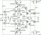
Are we talking about the same transistors? I meant the 2sc2240 and the 2sa970 on the top. I guess it's a sort of emitter follower then a VAS with a true cascode but the way it's folded to the second tail of the input pair is a little puzzling. And how does it react with the polarisation circuit with a constant current diode determining the cascode level for the fets? I guess I need to simulate it to fully get the principle. Quite unusual again... Anyone to comment? Maybe Lineup?
OH Sorry
It's a complimentary type current mirror circuit .
(This time�@may be not mistake . If I mistake,sorry)
It explains a similar circuit.
For the reference.
http://www.ne.jp/asahi/evo/amp/J200K1529/report.htm
[12]
Regard
It's a complimentary type current mirror circuit .
(This time�@may be not mistake . If I mistake,sorry)
It explains a similar circuit.
For the reference.
http://www.ne.jp/asahi/evo/amp/J200K1529/report.htm
[12]
Regard
Hello again,
Ok, I get the idea now about your DC nulling. I previously understood there was less DC left by this technic, it was not the point. Another way to do better with low frequencies while DC nulling is to use a fourth order filter instead of a second order, it's very effective. For the complementary mirror stuff, I get the idea now. It's something I never saw before, interesting... I learn everyday!
Ok, I get the idea now about your DC nulling. I previously understood there was less DC left by this technic, it was not the point. Another way to do better with low frequencies while DC nulling is to use a fourth order filter instead of a second order, it's very effective. For the complementary mirror stuff, I get the idea now. It's something I never saw before, interesting... I learn everyday!
Hello again turnA_zpoint and everyone,
I think I get your DC feedback scheme now:
When you add the input signal and the output signal and integrate them, it forms a feedforward/feedback DC error correction. The input signal is used as feedforward correction, while the output is used as feedback correction, and they are both added together in the inverting integrator...
Does this sound right?
Hi Rtarbell,
Thank you for the idea of an interesting viewpoint.
When interpreting it from another viewpoint,
this DC servo is LPF that referred to the input signal as it was,while a usual DC servo is LPF that refers to the ground line level.
Only Because ,the reference is different, I think that it differs from feedforward that I know. The feedforward that Iknow is the one with presumption and the process of operating it as for the result.
Please point it out if my idea is wrong.
Hi Wavebourn!
"but why output followers are powered from way higher voltage than a driver?"
Oh,it's only using my stock......😀
(there is no designing meaning...)
Regards!
Hi !
The OP LME49780 that Lineup taught ,I tried.(insead of LME49710)
It is a result in only in my condition.
I do not think a big difference to be.
But LME49780 is a little calm than LME49710 ,only my feeling.
Now I like LME79710 ,but according to circumstances, supply VOLT etc, LME49870 might come to like one.
both very good.
Thank you Lineup !
Regard !
Today's Test OPAMP
Hi
I tested OPAMP using input buffer (Now LME49710 is put it on) of this schematic, bellow
AD825,AD8065AR.( and OPA627AP again)
Still,LME49710 was the best sound .
Thank you.
Hi
I tested OPAMP using input buffer (Now LME49710 is put it on) of this schematic, bellow
AD825,AD8065AR.( and OPA627AP again)
Still,LME49710 was the best sound .
Thank you.
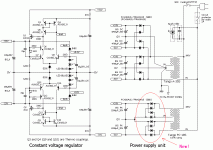
Today's tune
Hi!
I tune today the PSU.
+- sin wave each independence rectification.
This is a method of being so far.
The sin wave supplied to the home the distortion (a plus, a minus, sin wave is not same form)
So I does this tune to prevent the 0V of transformer to be influenced,.
I think it is necessary to treat same to the power output similarly originally. But for space factor , I tune only this.
I attach schematic.
Regard
Attachments
Hi
All guys
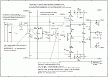
I report the result of PCB TEST of my AMP & Constant Vol Regulator.
http://www2.plala.or.jp/puthoff/amp5_PCB.html
<Outline>
The characteristic was steady by making to PCB.
Moreover, a new finding was obtained by the process of the test of
the Constant voltage power supply regulater circuit.
(1)AMP
Improve:
By making to PCB,The frequency response has improved. It might
be only an influence of the difference of part characteristics though
seems that this is because the wiring passing was shortened.
The phase amends one point.
The frequency response is 850KHz. (8ohm resistance load and 1W
output)
Inferior point:
Because PCB was installed in the radiator, the effect of
temperature change is large. The idling current of FET of the first
stage was thrown a lot so as not to become unstable when parts
were cold as measures. This was assumed to be future tasks.
(2)<Constant voltage power supply Regulator>
Point that understood this time:
The reason why the circuit starts has been understood even if it
supplies it from the output to which the current of the reference
supply is stabilized when the output is FET.
It is presumed that this is because the voltage is generated at the
gate by the action of the stray capacity between the drain and the
gate of FET when the output of the control circuit connected with
output FET is high impedance, and the current of the source of the
FET flows at power supply ON.
The circuit doesn't start because the voltage by the above-
mentioned stray capacity is not generated like the base of the
transistor when FET connects Daulington and for the bipolar
transistor.
Address of thanks
About the circuit editor and PCBCAD,
I use Free software distributed with "SUIGYODOU",
BSch3V and Minimal Board Editor(MBE).
http://www.suigyodo.com/online/
Thank you.
(Supplementation)
<Amplifier>
The circuit configuration is a reversing type amplifier of the current
return type that uses the transformer impedance circuit with the
gate earth circuit of FET to give the gain with the OP amplifier.
And the temperature amends circuit and the source resistance
were added and it was stabilized to the temperature change.
Because the hall diameter for MOS-FET of amplifier PCB is small, it
has expanded by the drill of 1.5mm in the diameter. Therefore,
soldering with the gate wiring, the drain, and the source is
reinforced.
This : because it scheduled to install it in the radiator at a position
away from MOS-FET at first.
(When MOS-FET is installed in PCB, the diameter need not be
expanded. )
<Constant voltage power supply Regulator circuit>
When the overcurrent was protected, the reference supply was
shutted down for the hunting cap prevention.
To experiment on several kinds of circuits, the part installation on
the back of the pattern cutting and PCB made it from assumption.
Regards
All guys
I report the result of PCB TEST of my AMP & Constant Vol Regulator.
http://www2.plala.or.jp/puthoff/amp5_PCB.html
<Outline>
The characteristic was steady by making to PCB.
Moreover, a new finding was obtained by the process of the test of
the Constant voltage power supply regulater circuit.
(1)AMP
Improve:
By making to PCB,The frequency response has improved. It might
be only an influence of the difference of part characteristics though
seems that this is because the wiring passing was shortened.
The phase amends one point.
The frequency response is 850KHz. (8ohm resistance load and 1W
output)
Inferior point:
Because PCB was installed in the radiator, the effect of
temperature change is large. The idling current of FET of the first
stage was thrown a lot so as not to become unstable when parts
were cold as measures. This was assumed to be future tasks.
(2)<Constant voltage power supply Regulator>
Point that understood this time:
The reason why the circuit starts has been understood even if it
supplies it from the output to which the current of the reference
supply is stabilized when the output is FET.
It is presumed that this is because the voltage is generated at the
gate by the action of the stray capacity between the drain and the
gate of FET when the output of the control circuit connected with
output FET is high impedance, and the current of the source of the
FET flows at power supply ON.
The circuit doesn't start because the voltage by the above-
mentioned stray capacity is not generated like the base of the
transistor when FET connects Daulington and for the bipolar
transistor.
Address of thanks
About the circuit editor and PCBCAD,
I use Free software distributed with "SUIGYODOU",
BSch3V and Minimal Board Editor(MBE).
http://www.suigyodo.com/online/
Thank you.
(Supplementation)
<Amplifier>
The circuit configuration is a reversing type amplifier of the current
return type that uses the transformer impedance circuit with the
gate earth circuit of FET to give the gain with the OP amplifier.
And the temperature amends circuit and the source resistance
were added and it was stabilized to the temperature change.
Because the hall diameter for MOS-FET of amplifier PCB is small, it
has expanded by the drill of 1.5mm in the diameter. Therefore,
soldering with the gate wiring, the drain, and the source is
reinforced.
This : because it scheduled to install it in the radiator at a position
away from MOS-FET at first.
(When MOS-FET is installed in PCB, the diameter need not be
expanded. )
<Constant voltage power supply Regulator circuit>
When the overcurrent was protected, the reference supply was
shutted down for the hunting cap prevention.
To experiment on several kinds of circuits, the part installation on
the back of the pattern cutting and PCB made it from assumption.
Regards
- Status
- Not open for further replies.
- Home
- Amplifiers
- Solid State
- Intro a circuit of study..