That not the point - the output when using a current mirror load - in the ideal world of a simulator the answer to the
question would be is zero current.
Good point, I must admit I overlooked that point.
Still the output of a current mirrored LTP is often taken as a voltage (with a buffered VAS), though fundamentally it does operate on current differential.
I still think for proper understanding one needs to analyze it's response to different inputs, or at least different polarities of input.
Just to be clear I'm not trying to argue. I concede your post was a sensible suggestion, and that such analysis will be beneficial to keantoken.
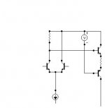
Okay, another good training for keantoken given the above diffamp circuit from sreten.
Given values:
-V = -6v
+V = +6v
all 3 resistors = 1k
V+In and V-In set to -1v
Now tell the currents through the 3 resistors, assuming Vbe of 0.7v.
Only allowed tool is calculator, no sims.
Mike
 You have the very spirit of a true teacher
 That not the point - the output when using a current mirror load is a current - in the ideal world of a simulator the answer to the
question would be is zero current.
Mikeks also calls the VAS as TIS (Transimpedance stage), current in, voltage out. I understand the voltage out part, because VAS gives the full voltage swing for the amp.
But what about the current input? Mikeks said that Miller cap makes the VAS receives current for high freq. AC signal.
Why the attached schematic works at all? MOSP is a mosfet, it is a voltage driven voltage. While the differential+current mirror that drives it gives current, not voltage? No miller cap there.
Attachments
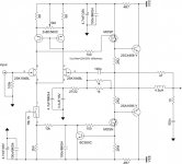
Lumanauw, this circuit works only because of the feedback adjusting the voltage to the mosfet. Open loop DC operation is undefined.
(Still have to wash away the wine from my screen...😀)
Outputvoltage will stay constant as long as diffamp has identical inputs on -IN and +IN. I estimate dominant pole to be at ... DC...
And openloop gain at DC ~INF. But that would make the amp oscillate at DC ??? I give up, funny circuit...
Mike
(Still have to wash away the wine from my screen...😀)
Outputvoltage will stay constant as long as diffamp has identical inputs on -IN and +IN. I estimate dominant pole to be at ... DC...
And openloop gain at DC ~INF. But that would make the amp oscillate at DC ??? I give up, funny circuit...
Mike
Hi, Mike,
I have a question about differental pair that uses current mirror for load.
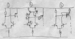
If the VAS is P-Mosfet, between 1,2,3, which one is the correct one to drive Pmosfet VAS?
Mike, could you help me with this?
In figure 2, point C is sitting between collector of current mirror (A) and drain of left differential (B).
Is this making point C = "High Impedance", because it is between 2 collectors? What is the approximation of impedance at point C?
If VAS is Pmosfet, then point D is also high impedance? Will this oscilate?
If VAS is bipolar, will it makes point D have low impedance? How low?
What is the "correct" connection between C and D? C=high impedance, D=low impedance, or C=low impedance, D=high impedance?
I have a question about differental pair that uses current mirror for load.
If the VAS is P-Mosfet, between 1,2,3, which one is the correct one to drive Pmosfet VAS?
Mike, could you help me with this?
In figure 2, point C is sitting between collector of current mirror (A) and drain of left differential (B).
Is this making point C = "High Impedance", because it is between 2 collectors? What is the approximation of impedance at point C?
If VAS is Pmosfet, then point D is also high impedance? Will this oscilate?
If VAS is bipolar, will it makes point D have low impedance? How low?
What is the "correct" connection between C and D? C=high impedance, D=low impedance, or C=low impedance, D=high impedance?
Attachments
+IN. I estimate dominant pole to be at ... DC...
And openloop gain at DC ~INF. But that would make the amp oscillate at DC ??? I give up, funny circuit...
Hi, Mike,
Oscilation at DC? What is the oscilation waveform looks like? 😀
Maybe it is not exactly DC, but 0.1hz?
Okay, but wait... Aren't the transistors negatively biased? Wouldn't this result in no current, or is this how you bias transistors in an LTP?
Assuming that the gain is 0, then the current through the supply would be 6V/((Rc1+Rc2)/2+Re)=4mA. This would be 2mA Ic through each transistor. With the input, assuming Vbe voltage drop to be 650mV, (-1V+.65V)/1k=-.35mA Ib. -.35mA*2 (for each transistor)=-.70mA, 4mA+-.70mA=3.3mA Ire. I suppose there would be some current running through the collector and out of the base, through the signal and into ground? I suppose you would calculate this by Irc-((-1V+.65)/Rc)=2mA--.35mA=2.35mA
So Irc1-2=2.35mA
Ire=3.3mA
The dreaded question: Am I right? *prepares for utter disapointment*
>>Mikeks also calls the VAS as TIS (Transimpedance stage), current in, voltage out.
you guys are funny the way you call the stages!!
a voltage amp is vin -- vout!!
john
you guys are funny the way you call the stages!!
a voltage amp is vin -- vout!!
john

Selamat Siang, David,
You know, I think people get really obsessive about the words. Is it transconductance, or transimpedance? Ah, the pain......
To get the VAS to work you have to push current in and out of it. The strict definition of transimpedance - current in, voltage out - would be pure current in, no voltage variation at all, and pure voltage out, doubtless at constant current.
The truth is the VAS is not pure transimpedance. You cannot get current in without a small voltage rise as well to drive that increase in current; it might only be a few mV, but one cannot exist without the other.
And who cares anyway? How does it improve the design if we can ascribe the correct word to the phenomenon?
Chars,
Hugh
I understand the voltage out part, because VAS gives the full voltage swing for the amp. But what about current input?
You know, I think people get really obsessive about the words. Is it transconductance, or transimpedance? Ah, the pain......
To get the VAS to work you have to push current in and out of it. The strict definition of transimpedance - current in, voltage out - would be pure current in, no voltage variation at all, and pure voltage out, doubtless at constant current.
The truth is the VAS is not pure transimpedance. You cannot get current in without a small voltage rise as well to drive that increase in current; it might only be a few mV, but one cannot exist without the other.
And who cares anyway? How does it improve the design if we can ascribe the correct word to the phenomenon?
Chars,
Hugh
Lumanauw, No1 and 3 will work normal. In No2 you are right, C represents an infinite output impedance, connected to a infinite high input impedance (D). This results in having an infinite voltage change at the slightest unbalance from the collector currents. (at dc)
Of course there is no such thing as infinite in real world, but close to.
There is an easy way out, simply put a resistor between the collectors of the diffamp.
Of course it does not oscillate, (i was having fun), the phasehift is not >180°, but is already 90° at the lowest freqs. This means, the amp you have shown acts completely as integrator throughout the audioband, beeing subject to PIM. (I don't know how pim sounds)
John, way wrong... Anything connected to a inf zout will become current in, the voltage there is only defined by the current flowing into that stage. For a bjt-vas, the ib to the vas-bjt is typically VERY unlinear, early effect, dynamic miller capacitance, varying hfe... This gives plenty of distortion...
Also, there is one vas type having nearly pure current in, folded cascode...
Keantoken, your "6V/((Rc1+Rc2)/2+Re)=4mA" is very wrong, as a hint, the sizes of Rc1/2 are not modifying the currents. Btw, your formula would give 3ma.
Please keep the bjts as infinite gain devices for now, having no Ib. Typically, Ib is small enough anyway to be ignored for simple bias calculations.
Understanding/seeing the currents & voltages in this diffamp example is absolutely fundamental, do not proceed with electronics before understanding this circuit. Once you worked that one out, you will have it much easier, believe me.
One more hint, using Vbe of 0.7v,the current through Re is 4.3ma, now try to understand why.
Kanwar, Rush cascode ?
Mike
Kanwar,
This is elegant beyond words.......
However, it has supernatural gain, and the feedback factor is too high, and moreover, there is no phase reversal, so you should run it from the feedback side, not the input side, and what about the overload latch?
I know you've solved all these problems, Kanwar, just stirring you up.......
Cheers,
Hugh
AKSA
sorry for this,but you are wrong.
All this circuit are non-inverting,so the output are in phase with the input and the NFB side are correct.
This circuit can have not a high open loop gain because the amount of total NFB can be set with degeneration resistors.
Another thing is strange for me : the connection emitter-emitter on the second transistors stage.......
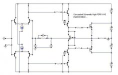
Workhorse said:Hi
look at this........
Kanwar, nice...
I would put those extra supplies on top of the output fets on gnd instead of on top of the output supplies. Otherwise, your output supply ripple will be replicated on top of the vas supply, and you don't want that, right?
Jan Didden
parsecaudio said:Another thing is strange for me : the connection emitter-emitter on the second transistors stage.......
But, that's what this is about... 🙄
Compared to normal vas, this arrangement is inverting and needs to be connected to the nfb side of diffamp, where the normal vas needs to be connected to the input side of diffamp...
On the "full" schematic Kanwar posted things are all right, Hugh refered obviously to the first small one.
Mike
Hi MikeB
.
The design are correct,with some little changes can be good,sure.
The connection emitter - emitter(i.e. low impedance that drive a low impedance) have at my advice not advantage in comparison to a classic cascode stage.
.
The design are correct,with some little changes can be good,sure.
The connection emitter - emitter(i.e. low impedance that drive a low impedance) have at my advice not advantage in comparison to a classic cascode stage.
- Status
- Not open for further replies.
- Home
- Amplifiers
- Solid State
- inquiries about LTP topology