The answer to that is probably that we should never approach clipping but yes, I think it has to sound worse under conditions where it is apparent such as on a sustained low organ pedal or something similar.
That's an interesting question, and one where the original design for this particular amp got it so wrong 😉
Post #21 and post #38 but read them all:
http://www.diyaudio.com/forums/soli...-lin-topology-nfb-tappings-2.html#post1623200
Another another concern is what happens when two amplifiers are attached to a common unregulated supply? There must be an interaction between the amplifiers.
That's an interesting question, and one where the original design for this particular amp got it so wrong 😉
Post #21 and post #38 but read them all:
http://www.diyaudio.com/forums/soli...-lin-topology-nfb-tappings-2.html#post1623200
Wrapping up the PSU sizing
Yes I will look at this in more detail. Douglas is also vocal about transformer sizing as well.
I am building Qty 4 mono P3A amplifiers. This exercise is to size the PSU and estimate expected performance. The P3A amplifier schematic is attached. A simple straight forward class AB amplifier which utilises bootstrapping. Been around for some time and is well tested. Expect to get about 50-60 watts max output.
The PSU is based on a Toroid transformer rated at 160 VA and 25-0-25 V output with 9% regulation. 4700uf electrolytic capacitors were used to smooth the bridge output.
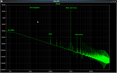
The FFT of the output with a 1.3V, 1 KHz test injected into the amplifier is attached. This gives a 5 mv DC offset, hum component about 80 DB below tone output and harmonic distortion below 0.01%. The amplifier is near clipping.
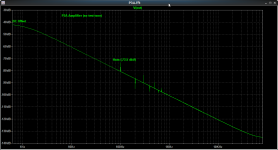
The FFT of the output when there is no test tone is also attached. This shows the hum component has dropped to -73.5 dbV. Tried an experiment nulling out the DC offset. It made the plot look pretty, but the hum component remained unchanged.
The predicted performance is more than adequate for my requirements. Perhaps a smaller toroid could be used. Unfortunately the transformers were wound today, so there is no going back. There is plenty of room in the amplifier enclosures, so 160 VA transformers easily fit. Wouldn't have saved much money either.
Tried larger smoothing capacitors, but it's not worth it. The simulation uses a slightly simplified schematic. The amplifier board will include more capacitors across the supply rails.
Rod Elliot measured the P3A hum output at -73 dbV. I don't know all the details of his setup, but the simulation is obviously close.
Now it's time to move onto selecting suitable speaker protection. And .. soon I can start soldering.
Thanks for the help...
That's an interesting question, and one where the original design for this particular amp got it so wrong 😉
Post #21 and post #38 but read them all:
http://www.diyaudio.com/forums/soli...-lin-topology-nfb-tappings-2.html#post1623200
Yes I will look at this in more detail. Douglas is also vocal about transformer sizing as well.
I am building Qty 4 mono P3A amplifiers. This exercise is to size the PSU and estimate expected performance. The P3A amplifier schematic is attached. A simple straight forward class AB amplifier which utilises bootstrapping. Been around for some time and is well tested. Expect to get about 50-60 watts max output.
The PSU is based on a Toroid transformer rated at 160 VA and 25-0-25 V output with 9% regulation. 4700uf electrolytic capacitors were used to smooth the bridge output.
The FFT of the output with a 1.3V, 1 KHz test injected into the amplifier is attached. This gives a 5 mv DC offset, hum component about 80 DB below tone output and harmonic distortion below 0.01%. The amplifier is near clipping.
The FFT of the output when there is no test tone is also attached. This shows the hum component has dropped to -73.5 dbV. Tried an experiment nulling out the DC offset. It made the plot look pretty, but the hum component remained unchanged.
The predicted performance is more than adequate for my requirements. Perhaps a smaller toroid could be used. Unfortunately the transformers were wound today, so there is no going back. There is plenty of room in the amplifier enclosures, so 160 VA transformers easily fit. Wouldn't have saved much money either.
Tried larger smoothing capacitors, but it's not worth it. The simulation uses a slightly simplified schematic. The amplifier board will include more capacitors across the supply rails.
Rod Elliot measured the P3A hum output at -73 dbV. I don't know all the details of his setup, but the simulation is obviously close.
Now it's time to move onto selecting suitable speaker protection. And .. soon I can start soldering.
Thanks for the help...
Attachments

Nice result 
You might find this useful, check out the 'app note 1' from the left hand menu:
The Signal Transfer Company
You might find this useful, check out the 'app note 1' from the left hand menu:
The Signal Transfer Company
I personally am a little nervous about the DC balance of the amplifier schematic in post #42. Reference voltage generator D1's current changes when the power supply voltage changes, and there is also unit-to-unit variability between different LEDs. So the voltage applied to the base of current sink transistor Q3 is just a bit unpredictable and Murphy's Law says that what you get is exactly what will injure you the most. So I would be inclined to replace fixed emitter resistor R7, with a 470 ohm resistor in series with a 20 turn, 200 ohm trimmer potentiometer. That way I could set the LTP current to be exactly the right number of milliamps, which produces exactly the right voltage drop across collector resistor R6, which produces exactly the right current in VAS transistor Q4, which gives zero DC offset at the output. {it might be convenient to short out C3 during measurement of DC offset; this magnifies the offset by 23X and makes it 23 times easier to measure}.
But the above is merely my own preference; others may prefer other approaches.
But the above is merely my own preference; others may prefer other approaches.
P3A Offset
Your concerns are valid. There are claims that LEDs sourced from different manufacturers will cause significantly different offsets in the amplifier output. Also, as you change the bias on the output devices the offset changes (in simulations).
I was thinking of replacing the led with a zener and adjusting R7 to a suitable value. Using a variable resistor as well seems to be worthwhile. These mods still retain the original design simplicity.
Will finish the build and see how it works. If necessary, will include modifications to allow manual setting of the offset. PCBs for this design have been sold for many years. No one seems to have come to grief yet.
I personally am a little nervous about the DC balance of the amplifier schematic in post #42. Reference voltage generator D1's current changes when the power supply voltage changes, and there is also unit-to-unit variability between different LEDs.
Your concerns are valid. There are claims that LEDs sourced from different manufacturers will cause significantly different offsets in the amplifier output. Also, as you change the bias on the output devices the offset changes (in simulations).
I was thinking of replacing the led with a zener and adjusting R7 to a suitable value. Using a variable resistor as well seems to be worthwhile. These mods still retain the original design simplicity.
Will finish the build and see how it works. If necessary, will include modifications to allow manual setting of the offset. PCBs for this design have been sold for many years. No one seems to have come to grief yet.
In the simulation you can replace the LED with a voltage source and see what the offset is over a wide range of values. It would give an idea of how compliant the design is.
A simple circuit like that (and bear in mind its target audience) would be acceptable and happy with a -/+100mv offset imo.
A simple circuit like that (and bear in mind its target audience) would be acceptable and happy with a -/+100mv offset imo.
P3A modifications
This amp design is the economy model. The objective is to maximize the performance without significant changes to the circuit topology or expense. ie tweaking a component here and there. You get some idea of this at http://www.diyaudio.com/forums/solid-state/164756-p3a-comparison-table-long.html#post2146744
The reasons for setting up the spice simulation was to investigate issues before the build is completed. It is apparent that a simple unregulated PSU will be sufficient. And I can use a locally manufactured transformer.
It would be nice to keep the offset of the output as low as possible. Possibly replace the LED with a zener and modify the emitter resistor to get a more accurate setting of offset . I'll keep in mind the comments contributed so far.
Maybe match the gain of the transistors in the LTP and thermally bond the two transistors. We'll see.
Unfortunately, unless I'm prepared to use a wooden housing it looks like the enclosure will have to come from Breeze Audio via Alibaba. That will keep the housing costs to around $100 to 120 AUD. A good enclosure will help keeping the overall build neat and tidy. (My last build the ETI 480 was a triumph of sculpture over technology. As components fell off they would be soldered back on again. Only had to replace fuses on the rails a couple of times. It lasted for 20 years and now is to be replaced with multiple amplifiers.)
It's probably appropriate for me to submit further queries across to thread in the Solid State forum. We aren't discussing the PSU anymore.
A simple circuit like that (and bear in mind its target audience) would be acceptable and happy with a -/+100mv offset imo.
This amp design is the economy model. The objective is to maximize the performance without significant changes to the circuit topology or expense. ie tweaking a component here and there. You get some idea of this at http://www.diyaudio.com/forums/solid-state/164756-p3a-comparison-table-long.html#post2146744
The reasons for setting up the spice simulation was to investigate issues before the build is completed. It is apparent that a simple unregulated PSU will be sufficient. And I can use a locally manufactured transformer.
It would be nice to keep the offset of the output as low as possible. Possibly replace the LED with a zener and modify the emitter resistor to get a more accurate setting of offset . I'll keep in mind the comments contributed so far.
Maybe match the gain of the transistors in the LTP and thermally bond the two transistors. We'll see.
Unfortunately, unless I'm prepared to use a wooden housing it looks like the enclosure will have to come from Breeze Audio via Alibaba. That will keep the housing costs to around $100 to 120 AUD. A good enclosure will help keeping the overall build neat and tidy. (My last build the ETI 480 was a triumph of sculpture over technology. As components fell off they would be soldered back on again. Only had to replace fuses on the rails a couple of times. It lasted for 20 years and now is to be replaced with multiple amplifiers.)
It's probably appropriate for me to submit further queries across to thread in the Solid State forum. We aren't discussing the PSU anymore.
Fair enough 🙂 It sounds like you are planning and researching this one thoroughly which is good. Matching the gain of the LTP can only be a good thing, close thermal bonding perhaps less important in the whole scheme of things if its all boxed up in a case. That said, if the board layout lends itself then yes, thermally couple as well.
Hi
I think that the HUM is caused by the fact that C3 should be connected to R2 and then C3 & R2 to ground. The BIAS transistor may need a collector to base cap and full bypass collector to emitter to keep it stable. The layout is very important to the total performance of the amplifier. Good hunting.
Duke 🙂
- Status
- Not open for further replies.
- Home
- Amplifiers
- Power Supplies
- Incredibly dumb LTspice question: simulating amp load for PSU