Carlos,
that's what I planned, anyway. I just thought that you might have something up the sleeve considering the time and effort you invested in snubber applications.
As for UNO, I don't presume it can beat your AD815 pre (I built it and I enjoy it, thank you once again). It's just that UNO is so sweet and simple that I might give it a try.
Cheers !
juma said:Carlos,
that's what I planned, anyway. I just thought that you might have something up the sleeve considering the time and effort you invested in snubber applications.
As for UNO, I don't presume it can beat your AD815 pre (I built it and I enjoy it, thank you once again). It's just that UNO is so sweet and simple that I might give it a try.
Cheers !
That's right, the UNO is just too good for what it is, that's it.
Build it, I would like to know your oppinion.
It has a snubber.


LT1083
For the last ten days I've been trying to implement LT1083 as regulator for Carlos' NIGC, actually to find snubber values that would make it sound at least as good as unreg. snubbered, but without succes. It just doesn't seem possible to get that GC midband magic out of LT1083.
33nf in parallel with 0R33+33uF on the output of LT1083 are the best shot, but mids (especially voices and strings still sound like performers stepped 1 meter back from the microphone). At the same time bass started to get bigger volume and deeper blow with same control it had previously, which happened no matter what snubber combination I used.
It looks like that LT1083 would have done well in bi-/tri-amping system (PSU for bass amp).
I'll keep on trying (shame to waste such expensive devices), but not many tricks are left in the box.
Cheers
LT1083 - problem solved
Well, as it happens sometimes in life, I was looking for for solution on the wrong place. There is nothing wrong with LT1083 (au contraire). The problem was in coupling cap between AD815 preamp and power amp (3,3 uF Siemens, industrial type MKT).
Having no Black Gates on hand (and not being ready to pay 40 EURO for a single 3,3uF cap, even if it's made from fairy dust and unicorn's tears), I decided that no cap is best cap and went for direct coupling.
Since AD815 has 30mv DC offset on its output it is obvious that LM3886 should have unity gain for DC, so Ci came back in play as 220uF//4,7uF Wima//100nF MKP in series with 200 Ohm as Ri and 4K3 as Rf.
And yes, Ci made this way affects the overall sound much, much less than it does usually (coupling cap in direct signal path does a lot more damage, magical or not).
And now, sound is right, everything is as it should be, all benefits of standard Carlos' circuit are present, plus benefits in bass that I mentioned in previous post (and improvements descended from using a regulated PSU in this integrated amp).
One thing should be kept in mind: the source component (CD/DVD player, DAC, PC sound card, whatever) should have no significant DC offset voltage on its output (up to 20 mV is OK) in order to keep it under 100mV on the speaker.
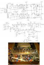
Attached is schematic and picture of amp (built p2p of course).
Cheers
Well, as it happens sometimes in life, I was looking for for solution on the wrong place. There is nothing wrong with LT1083 (au contraire). The problem was in coupling cap between AD815 preamp and power amp (3,3 uF Siemens, industrial type MKT).
Having no Black Gates on hand (and not being ready to pay 40 EURO for a single 3,3uF cap, even if it's made from fairy dust and unicorn's tears), I decided that no cap is best cap and went for direct coupling.
Since AD815 has 30mv DC offset on its output it is obvious that LM3886 should have unity gain for DC, so Ci came back in play as 220uF//4,7uF Wima//100nF MKP in series with 200 Ohm as Ri and 4K3 as Rf.
And yes, Ci made this way affects the overall sound much, much less than it does usually (coupling cap in direct signal path does a lot more damage, magical or not).
And now, sound is right, everything is as it should be, all benefits of standard Carlos' circuit are present, plus benefits in bass that I mentioned in previous post (and improvements descended from using a regulated PSU in this integrated amp).
One thing should be kept in mind: the source component (CD/DVD player, DAC, PC sound card, whatever) should have no significant DC offset voltage on its output (up to 20 mV is OK) in order to keep it under 100mV on the speaker.
Attached is schematic and picture of amp (built p2p of course).
Cheers
Attachments
carlosfm said:Another satisfied customer. 😎
I suppose the satisfaction is mutual, since you've been sharing freely results of yous efforts (I don't remember Carlos tried to sell anything on this forum). And the end result is as it should be: more people are building good amps and listening to the music in a more joyful manner.
Thanks Carlos !
And here is a web page that I stumbled upon (let's share some laughs too). I don't remember when was the last time I laughed so much - be careful, this can lead to serious injuries :
http://www.dself.dsl.pipex.com/ampins/failproj/failproj.htm
Cheers
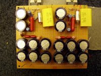
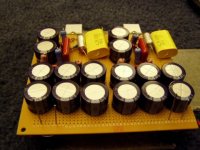
Finished the board for the non-verting power amp today. I listened for about five minutes,it sounds OK. I will burn it in for 3 days and give it another listen.
It is a little different from Carlos' schematic. I didnt have all the parts for the snubbers.so the values are different. I used .33ohm and a 1nf cap instead of .1ohm resistor and 3.3nf cap. The power supply snubber components are the same as schematic's
I also used a 4.7uf cap bypass with a polystylene,I dont know if it help but I brought 150pcs,so I will use them someplace.
Attachments
Technically, a schematic only shows the logical connections between components not the physical layout. When you read your schematics, your brain automatically sees it as a physical layout, others that have not build one or two hundred GC and PSU may not make this translation....
I am a total newb to making electronics, but I had the exact same thought as that quoted. Is there any reason why I should NOT try to lay out the components physically as closely as possible to the schematic layout? The schematic looks like a blueprint so why not use it, as much as possible, like a blueprint for perfboard layout and soldering? I was going to note a possible exception (or need for insulation) where lines cross without a solid dot, but there are no such crossings. Is that perhaps all the more reason to view the schematic as both a logical and physical layout/blueprint/map?
I'm a complete newb to making electronics. The schematic seems clear enough, but I have some trouble understanding one or more of the 4 comments re snubbering. All help will be greatly appreciated.
1. "Use 2,2000uf + 100nF (*) on the chip's PSU pins." Presumably this means pins 9 & 10 on the LM3886. Does this mean that I should run the resistor & capacitor between pins 9 and pin 10? Do I do it twice, first in the order pin9-resistor-capacitor-pin10 and then in the order pin10-resistor-capacitor-pin9?
2. "3.3uF(*) from V+ to V- pins." Presumably this means pins 1&5 and 4 on the LM3886. Does this mean that, after connecting pins 1 & 5, I should run the resistor & capacitor between pins 1/5 and pin 4? Do I do it twice, first in the order pins1/5-resistor-capacitor-pin4 and then in the order pin4-resistor-capacitor-pin1/5?
3. "0.1R/1W + 3.3nF(*) snubber just before these caps." I don't understand the "just before" bit relative to caps connected to LM3886 pins. Assuming I have soldered the resistor and capacitor together, where do I attach the other ends of the resistor and capacitor? Do I need to do it twice, first in one direction then in the other? Is there a schematic or showing where the connections are made?
4. "(*) Use small 100V MKT caps." I see asterisks in 5 places; 3 in the comments above, 2 beside C9 & C10 (both 1.5nF). What does "MKT" mean? Do all 5 capacitors come rated for 100V?
All help would be greatly appreciated.
Pins 9 and 10 are the inputs, not supply. pins 1+5 are V+, pin 4 is V-. Supply rails are decoupled to ground with capacitors, near the chip. The suggestion is 2.2mF electrolytic and 100nF ceramic in parallel for this decoupling. Suitably voltage rated of course. No resistors are involved.I'm a complete newb to making electronics. The schematic seems clear enough, but I have some trouble understanding one or more of the 4 comments re snubbering. All help will be greatly appreciated.
1. "Use 2,2000uf + 100nF (*) on the chip's PSU pins." Presumably this means pins 9 & 10 on the LM3886. Does this mean that I should run the resistor & capacitor between pins 9 and pin 10? Do I do it twice, first in the order pin9-resistor-capacitor-pin10 and then in the order pin10-resistor-capacitor-pin9?
Another decoupling cap between supplies, no resistor involved.2. "3.3uF(*) from V+ to V- pins." Presumably this means pins 1&5 and 4 on the LM3886. Does this mean that, after connecting pins 1 & 5, I should run the resistor & capacitor between pins 1/5 and pin 4? Do I do it twice, first in the order pins1/5-resistor-capacitor-pin4 and then in the order pin4-resistor-capacitor-pin1/5?
RC snubber on power rail between chip and the main decoupling. As in the diagram in post #244. Direction is immaterial for series connected R and C.3. "0.1R/1W + 3.3nF(*) snubber just before these caps." I don't understand the "just before" bit relative to caps connected to LM3886 pins. Assuming I have soldered the resistor and capacitor together, where do I attach the other ends of the resistor and capacitor? Do I need to do it twice, first in one direction then in the other? Is there a schematic or showing where the connections are made?
Google can answer questions like what is an "MKT capacitor": polyester film.4. "(*) Use small 100V MKT caps." I see asterisks in 5 places; 3 in the comments above, 2 beside C9 & C10 (both 1.5nF). What does "MKT" mean? Do all 5 capacitors come rated for 100V?
All help would be greatly appreciated.
- Home
- Amplifiers
- Chip Amps
- Improving the Non-Inverting chipamp