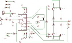
Sup! i was going to make the pcb for this schematic but im not sure if it will work the right way.
i was wondering if you guys could look at it and tell me whats wrong and how to fix it.
the out put transistors are not going to be the tip142 and 147 but some thing like tip35CW and tip36cw or the mjl1302ag and mjl3281ag,
do you think i need a predriver for each of the output stage drivers. or just one pair of predrivers to push the 2 pair of output drivers.
for predrivers i have the mje15032g and mje15033g and a set of bdx54c and bdx53c, thanks for the help in advance.
laters all.
i had to change the image type from bmp to jpeg.
Attachments
Looks pretty close to the circuit in the datasheet. Couple things to keep in mind. First is that you will need to optimize values for your particular PCB layout and design. So you should do somethings to have lots of flexibility to work with unless you are experienced enough to kick out a PCB that will work the way you want. Some things to be sure to have:
- 0.1uF capacitor at supply pin of each output device.
- snubber on the output, 0.1uF + 10ohms are good starting values
- Extra driver stage may or may not be needed depending on final output devices, supply voltage and load impedance. You can add places for these and then jumper them out if they are not needed.
- Compensation cap (10pF) will probably need to be higher to start then you can optimize down once you are sure you have stability.
- Add a couple cap footprints across the bias pins, I use a film cap and a small electrolytic. You can play with values and combinations to see what you like.
- Add a cap footprint from the Mute pin to GND depending on if you plan to use the Mute function. A capacitor here will insure no pops going in/out of Mute. If not using Mute mode then don't worry about it.
- You might want to add L+R on the output. Might not be needed.
Good luck.
-SL
thanks for the reply SpittinLLama!
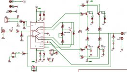
My electronics lingo is not so good, so i hope i understood what you where saying. here is what i changed based on your suggestions, plz let me know if the changes i made, was what you suggested.
im new to electronics so i can really use all the info you can help with, thanks again.
*added C8 trough C11 to the collector side of the transistors to ground. I hope thats what you meant, please correct me if i messed up. would 100uF work as well?
*added R1 and C11 .1uF caps.
*i want this amp to be slightly flexible as far as power rating goes.
so ill add the spaces for a pre driver stage and two more spot for the output drivers. and jumper the unused.
*The power supply i made its a +/-60V unregulated output.
the transformer was pulled from a jvc home 5.1 receiver amp.
the voltage drops to 45v under a 11ohms load at 4.5 amps, so around 200wrms to work with.
*I'm looking to drive from 16ohms to hopefully 4ohms loads.
*The amp will be used for bi amping a pair of 3 way towers.
*would 30pf be too big, what would be a range? if you know.
*Added CC1 its a 30pf from one bias pin to the other. " Not sure if thats how you meant it!" what would be a general value for the film cap?.
* i do want to use the mute option. So like you said i added a .1uF from the pin to ground. is that right? what do you mean by footprint?
thanks a bunch.
take care.
l8ter
My electronics lingo is not so good, so i hope i understood what you where saying. here is what i changed based on your suggestions, plz let me know if the changes i made, was what you suggested.
im new to electronics so i can really use all the info you can help with, thanks again.
- 0.1uF capacitor at supply pin of each output device.
*added C8 trough C11 to the collector side of the transistors to ground. I hope thats what you meant, please correct me if i messed up. would 100uF work as well?
- snubber on the output, 0.1uF + 10ohms are good starting values
*added R1 and C11 .1uF caps.
- Extra driver stage may or may not be needed depending on final output devices, supply voltage and load impedance. You can add places for these and then jumper them out if they are not needed.
*i want this amp to be slightly flexible as far as power rating goes.
so ill add the spaces for a pre driver stage and two more spot for the output drivers. and jumper the unused.
*The power supply i made its a +/-60V unregulated output.
the transformer was pulled from a jvc home 5.1 receiver amp.
the voltage drops to 45v under a 11ohms load at 4.5 amps, so around 200wrms to work with.
*I'm looking to drive from 16ohms to hopefully 4ohms loads.
*The amp will be used for bi amping a pair of 3 way towers.
- Compensation cap (10pF) will probably need to be higher to start then you can optimize down once you are sure you have stability.
*would 30pf be too big, what would be a range? if you know.
- Add a couple cap footprints across the bias pins, I use a film cap and a small electrolytic. You can play with values and combinations to see what you like.
*Added CC1 its a 30pf from one bias pin to the other. " Not sure if thats how you meant it!" what would be a general value for the film cap?.
- Add a cap footprint from the Mute pin to GND depending on if you plan to use the Mute function. A capacitor here will insure no pops going in/out of Mute. If not using Mute mode then don't worry about it.
* i do want to use the mute option. So like you said i added a .1uF from the pin to ground. is that right? what do you mean by footprint?
thanks a bunch.
take care.
l8ter
Attachments
Hi,
a dual EF output stage requiring drivers is recommended.
The C1=0.47uF input cap will kill the bass performance.
Add an RF filter to the input. C//RS, about 1nF will do.
Why is Rin=243r so low?
a dual EF output stage requiring drivers is recommended.
The C1=0.47uF input cap will kill the bass performance.
Add an RF filter to the input. C//RS, about 1nF will do.
Why is Rin=243r so low?
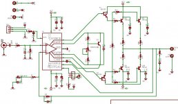
Hi AndrewT, thanks for the reply.
i guess ill be using the EF stage to push the output stage. do you know if these devices i have would be worth using as predrivers? mje15032g and mje15033g and a set of bdx54c and bdx53c,
MJE15032G Datasheet
BDX54C Datasheet
they'll have to drive a set of either one of these tip35CW and tip36cw or the mjl1302ag and mjl3281ag,
MJL1302AG Datasheet TIP36CW Datasheet
added a 1nF cap in parallel to the rs resistor. is that what you meant?
" For best Noise performance, lower values of resistors are
used. A value of 243 is commonly used for Ri "
ill play with other values ones the pcb is built, to see how performance changes. any suggestions?
thanks again.
any more help on this will be greatly appreciated.
laters
a dual EF output stage requiring drivers is recommended.
i guess ill be using the EF stage to push the output stage. do you know if these devices i have would be worth using as predrivers? mje15032g and mje15033g and a set of bdx54c and bdx53c,
MJE15032G Datasheet
BDX54C Datasheet
they'll have to drive a set of either one of these tip35CW and tip36cw or the mjl1302ag and mjl3281ag,
MJL1302AG Datasheet TIP36CW Datasheet
true thanks. i changed it for a 220uF. is that enough. I cant get the equation formula to work for me.The C1=0.47uF input cap will kill the bass performance.
\Add an RF filter to the input. C//RS, about 1nF will do.
added a 1nF cap in parallel to the rs resistor. is that what you meant?
on the LME application PDF i quote.Why is Rin=243r so low?
" For best Noise performance, lower values of resistors are
used. A value of 243 is commonly used for Ri "
ill play with other values ones the pcb is built, to see how performance changes. any suggestions?
thanks again.
any more help on this will be greatly appreciated.
laters
Attachments
Hi,
input impedance of 6k8 + 243r~=7k is a bit low.
Ci=220uF is far too large. This cap must define the high pass rolloff.
Use about 1u5F or 1u8F with your original 22k for Rs. These should match <=time constant of the NFB/1.4
You could try Rin between 243r and 750r, any higher and you will probably notice the treble rolling off.
AndrewT said:Hi,
input impedance of 6k8 + 243r~=7k is a bit low.
Ci=220uF is far too large. This cap must define the high pass rolloff.
Use about 1u5F or 1u8F with your original 22k for Rs. These should match <=time constant of the NFB/1.4
You could try Rin between 243r and 750r, any higher and you will probably notice the treble rolling off.
sup!
i think i made the changes you mentioned above, im not sure if they are in the right place though.
for the input stage on the LME would the filtering work the same way as if i was adding a filter to an opamp?
thanks for the help so far.
laters
An externally hosted image should be here but it was not working when we last tested it.
Sup all!
well i guess there is really not much else to change to make it operational.
if you guys have any more tips for the amp, please help me out.
ill play with some of the values once the PCB is done and the amp working.
here is the last schematic and PCB.
ill provably make the board tomorrow or the next day.
if you see anything i could change to improve, im sure theres allot of room for improvement here, lol, feel free to help
thanks
laters
well i guess there is really not much else to change to make it operational.
if you guys have any more tips for the amp, please help me out.
ill play with some of the values once the PCB is done and the amp working.
here is the last schematic and PCB.
An externally hosted image should be here but it was not working when we last tested it.
An externally hosted image should be here but it was not working when we last tested it.
ill provably make the board tomorrow or the next day.
if you see anything i could change to improve, im sure theres allot of room for improvement here, lol, feel free to help
thanks
laters
Sup all!
i came up with a new pcb for the amp, felt this one would be a bit more appropriate, i still have to correct all the traces width according to what ever current they will carry.
do you think the location of the transistors is better on the previous post PCB or this one?
The Heatsink i have on hand is a 12" x 5 3/8" flat contact surface. i want to use the heat sink to its max,
would it be posible to attach 4 of these amps to this heat sink?
would the 2SC3063 npn transistor work fine for the vbe multiplier?.
here is the 2SC3063 Datasheet
laters
i came up with a new pcb for the amp, felt this one would be a bit more appropriate, i still have to correct all the traces width according to what ever current they will carry.
An externally hosted image should be here but it was not working when we last tested it.
An externally hosted image should be here but it was not working when we last tested it.
do you think the location of the transistors is better on the previous post PCB or this one?
The Heatsink i have on hand is a 12" x 5 3/8" flat contact surface. i want to use the heat sink to its max,
would it be posible to attach 4 of these amps to this heat sink?
would the 2SC3063 npn transistor work fine for the vbe multiplier?.
here is the 2SC3063 Datasheet
laters
Hi Boricuaso,
Any success on your amp? I'm just curios how did it sound, or have you compared it on your existing amps based on the sound quality? What is your trim bias current of your amp? Can you show me know where to point my multimeter leads on measuring the bias?
Any success on your amp? I'm just curios how did it sound, or have you compared it on your existing amps based on the sound quality? What is your trim bias current of your amp? Can you show me know where to point my multimeter leads on measuring the bias?
fredlock said:Hi Boricuaso,
Any success on your amp? I'm just curios how did it sound, or have you compared it on your existing amps based on the sound quality? What is your trim bias current of your amp? Can you show me know where to point my multimeter leads on measuring the bias?
Hi, sorry for the lack of reply, i have changed the schematic and PCB once more before i started building it, i just didn't post the changes,but ill post the changes before the weekend starts. the components in front of the V+ pad are the bias components, there is one cap, two resistors and one trimer at the far right of those comps, if you follow the tracks coming from the trim pot you'll find the transistor, just a bit above it. you can measure the bias there or if you prefer at the pot. im not done building it yet, so i don't know how it sounds, im sure ill have to tweak and replace a couple more components, before i can find out the final outcome on sound Q. laters
design update
Sup all, here is my new schematic and PCB for this project, if anyone could give it a look and let me know if there is anything that should be changed or fixed that would be super great. im still assembling the amp, so it'll be a couple more days before i fire it up, so i can still make changes to it before it catches on fire, lol. any help is highly appreciated. the images are links to a better version of the same image, with an option for the full Size image, for much better quality image.
Thanks.
Sup all, here is my new schematic and PCB for this project, if anyone could give it a look and let me know if there is anything that should be changed or fixed that would be super great. im still assembling the amp, so it'll be a couple more days before i fire it up, so i can still make changes to it before it catches on fire, lol. any help is highly appreciated. the images are links to a better version of the same image, with an option for the full Size image, for much better quality image.
An externally hosted image should be here but it was not working when we last tested it.
An externally hosted image should be here but it was not working when we last tested it.
An externally hosted image should be here but it was not working when we last tested it.
Thanks.
HI!, well im going to power the amp today or tomorrow and was wondering if there is a proper way for me to do this, like using half the supply voltage, etc.. i just want to find out before hand a couple of ways of keeping my amp from burning up on the first try, while im tweaking it to get it running properly. Any help is highly appreciated.
each time you power up a new or modified mains project use a mains light bulb (40W to 100W) in series with the live feed.boricuaso said:HI!, well im going to power the amp today or tomorrow and was wondering if there is a proper way for me to do this, like using half the supply voltage, etc.. i just want to find out before hand a couple of ways of keeping my amp from burning up on the first try, while im tweaking it to get it running properly. Any help is highly appreciated.
AndrewT said:each time you power up a new or modified mains project use a mains light bulb (40W to 100W) in series with the live feed.
HI! do you mean like at the output of the amplifier or at the power supply to lower the voltage or current going to the amplifier rails?
i was planing on using a -+20volts or maybe a -+15volts while i adjust the bias, the gains and the resistors for the transistors base.
then raising the voltage slightly till everyting works with -+60volts.
thanks for the help so far.
let me know what you think i should do.
No
a mains light bulb in series with the live feed to the equipment.
If the new project draws too much current, due to a wiring error , the bulb filament heats up and almost instantly increases it's resistance to reduce the mains voltage fed to the project. This ensures that explosive results cannot occur.
It often prevents any damage while you scratch your head wondering why the bulb does not go out and allows measurements to be taken in troubleshooting the problem.
Andrew T, would this apply to any amplifier projects under test, connecting a light bulb in series to the main AC lines of the amp? I know it's an old school procedure but I think very effective.
AndrewT said:No
a mains light bulb in series with the live feed to the equipment.
If the new project draws too much current, due to a wiring error , the bulb filament heats up and almost instantly increases it's resistance to reduce the mains voltage fed to the project. This ensures that explosive results cannot occur.
It often prevents any damage while you scratch your head wondering why the bulb does not go out and allows measurements to be taken in troubleshooting the problem.
thanks allot, i finaly get it.
thats is a pretty cool way to protect the amp while i adjust and tweak.
ill post in a couple of hours, with the good or the bad results. lol
thanks again AndrewT you're a big help.
laters
mains light bulb tester
I recommend that each new project is first powered up through the bulb and every time you modify the project, again power up through the bulb
always.fredlock said:would this apply to any amplifier projects under test, connecting a light bulb in series to the main AC lines of the amp?
I recommend that each new project is first powered up through the bulb and every time you modify the project, again power up through the bulb
the amp was working fine with the light bulb, once i took the bulb off the amp when up in smoke in a couple of seconds. im still trying to figure out what happened. all the pins on the transistors measure the same as the rail voltage +-45V , so i guess they need to be replaced. same for the source and sink pin on the LME, i should of used a heat sink on the LME, it was running cool with the bulb in, so i figure it didnt need it, guess i was wrong.
im making a new board with everything rearranged for the better. i wasnt too happy with the track width and transistor placement on that last one.
what would be a decent transistor to use for the bias?
what value should i use for the resistor at the base of the driver transistors. although it was on the schematic, i didn't use it on the amp.
maybe thats one reason why it burnt out. maybe not.
any help on that, would be great.
laters
- Status
- Not open for further replies.
- Home
- Amplifiers
- Chip Amps
- i need help with this LME49810 schematic