Is this because you mirrored them on the schematic or they were simply wrong to begin with? (I picked up and used the same part in my other project.)
Is this because you mirrored them on the schematic or they were simply wrong to begin with? (I picked up and used the same part in my other project.)
This is not because it is mirrored. It is because it was the wrong way in the beginning (only pins 3 & 4 are mixed). I'm sorry about that, my mistake..
No problem. I'm a while away from going to boards. I just grabbed the LTV816S device as you had done and renamed it (mirroring it on the schematic as you done). I'm just thinking about how I can make the necessary change. I'm away from my desk at the moment but do I need to swap pins 3 and 4 or is the LTV816S pinned correctly for the VOM1271?
I'm away from my desk at the moment but do I need to swap pins 3 and 4 or is the LTV816S pinned correctly for the VOM1271?
Yes, pin swapping is all you need to do to make it correct..
Last edited:
This is going to be the adapter to swap pins 3 & 4:
An externally hosted image should be here but it was not working when we last tested it.
I received the boards yesterday. They have very nice quality:
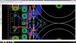
Unfortunately, I spotted a nasty mistake on my board layout, which prevents using the auto-on circuitry properly. This image shows the error:
I'll just connect the other end of R16 directly to the "/ON" wire and not through the pad.
An externally hosted image should be here but it was not working when we last tested it.
An externally hosted image should be here but it was not working when we last tested it.
Unfortunately, I spotted a nasty mistake on my board layout, which prevents using the auto-on circuitry properly. This image shows the error:
An externally hosted image should be here but it was not working when we last tested it.
I'll just connect the other end of R16 directly to the "/ON" wire and not through the pad.
I'm surprised too. Now I run the DRC check again and I suddenly found a few more stupid mistakes 😱Good luck. I'm surprised a DRC check didn't uncover that one.
I managed to fix the errors on the board:
An externally hosted image should be here but it was not working when we last tested it.
I received the boards yesterday. They have very nice quality:
Unfortunately, I spotted a nasty mistake on my board layout, which prevents using the auto-on circuitry properly. This image shows the error:
An externally hosted image should be here but it was not working when we last tested it.
I'll just connect the other end of R16 directly to the "/ON" wire and not through the pad.
What a shame and strange , looks fine on my Eagle ( see attachment )
Cheers ,
Rens
Attachments
I think you are looking at the new version. I have the version Piisami posted awhile ago and the error is there in Eagle. Doesn't look like the errors were insurmountable.
Last edited:
I'm still intrigued as to the the decision to use the VOM1271. Dan had said in the thread discussing my languishing project that "for power amplifier circuits like Piisami's, there is a need to break supply lines of both polarities simultaneously, and with fairly substantial currents and volts." Is it simply "simultaneously" which drove this choice?
Actually I think I am slowly, painfully understanding the answer to my question above. I had always thought of the VOM1271 as simply presenting, say, 8.5V (with c25mA of current across the LED) to the gate of the MOSFET (i.e. 8.5V ref to ground). I had also thought that the use of a photovoltaic IC was due to a desire for isolation.)
I now understand the challenge with a high-side switch is finding a voltage to present to the gate of the MOSFET that is at least Vgs(th) above the rail voltage. I had simply been thinking of Vgs and Vgs(th) as levels referenced to GND/0v.
I now see, if I am not still mistaken, the VOM1271 drives the Vgs of the MOSFET i.e. if the output voltage of the rail is 55V, 25mA of 5V on the LED side of the VOM1271 will mean the a 'gate voltage' of 63.5V for a Vgs of 8.5v.
Does this make sense or am I going completely looney?
Dan had said ...
It's Dave, well David actually😉
Actually I think I am slowly, painfully understanding the answer to my question above. I had always thought of the VOM1271 as simply presenting, say, 8.5V (with c25mA of current across the LED) to the gate of the MOSFET (i.e. 8.5V ref to ground). I had also thought that the use of a photovoltaic IC was due to a desire for isolation.)
I now understand the challenge with a high-side switch is finding a voltage to present to the gate of the MOSFET that is at least Vgs(th) above the rail voltage. I had simply been thinking of Vgs and Vgs(th) as levels referenced to GND/0v.
I now see, if I am not still mistaken, the VOM1271 drives the Vgs of the MOSFET i.e. if the output voltage of the rail is 55V, 25mA of 5V on the LED side of the VOM1271 will mean the a 'gate voltage' of 63.5V for a Vgs of 8.5v.
Does this make sense...
Absolutely. That was the main point.
It was also what my first comment to you was about, that the photovoltaic "floats" the Vgs.
Once you have photovoltaic on one side it is then simplest to duplicate on the other.
This then eliminates any risk of problems from imbalanced power supply if the two sides were to turn on or off at different rates.
Best wishes
Dave
Last edited:
Whoops, sorry David - not sure how that happened. Yeah, but because I was just thinking of voltages with reference to ground I was thinking a source voltage for the gates of, say, 5v was plenty. Of course when I modeled things out I realized my error. An incredibly basic one. The fact that the VOM1271 is photovoltaic is somewhat coincidental. I was thinking it was related to isolation albeit the common ground gave me serious doubt this was correct. It wasn't until I dropped it and tried to model a high side switch with NMOS load switches that I fully understood its role. So...the problem requires high side load switches which can be done with PMOS transistors and no additional voltage source or NMOS transistors, an additional voltage source and a driver to 'float' Vgs. If one is sensitive to Rds(on) which is particularly an issue if rail currents are high, one is forced to use the latter. Got it. Finally.
Picaxe 08M2
Chips are programmed and send .
As I have no VOM's I tested the Picaxe chip for all fault conditions .
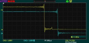
The DC error works pretty fast , average was below 200 uSec .
I attached a scope picture of the worst timing I measured , around 280 uSec after the DC error goes low , Pin1 on the Picaxe goes low so the Fets will close . Had some problems with the High side DC detection at first , but discovered that pin2 of the Picaxe is not TTL logic , but Schmitt Trigger compatible , this means that a Logic high must be >4Volt .
I will post a little Excel sheet to calculate the proper resistor divider values for the supply rails later .
The Picaxe code is shown below .
Yellow in the picture is the DCerr signal and Blue is the Voltage on pin1 Picaxe
Cheers ,
Rens
Chips are programmed and send .
As I have no VOM's I tested the Picaxe chip for all fault conditions .
The DC error works pretty fast , average was below 200 uSec .
I attached a scope picture of the worst timing I measured , around 280 uSec after the DC error goes low , Pin1 on the Picaxe goes low so the Fets will close . Had some problems with the High side DC detection at first , but discovered that pin2 of the Picaxe is not TTL logic , but Schmitt Trigger compatible , this means that a Logic high must be >4Volt .
I will post a little Excel sheet to calculate the proper resistor divider values for the supply rails later .
The Picaxe code is shown below .
Code:
          low C.1                                     ; Fets closed
          setfreq m32                               ; chip clock 32Mhz
          for b0 = 1 to 10                         ; 10 sec delay LED flashes 2Hz                           high C.0
          pause 4000
          low C.0
          pause 4000
          next

          if pinC.2 = 1 then goto FetF    ; check if Pos Fet is open
          if pinC.4 = 0 then goto FetF    ; check if Neg Fet is open
          high C.0                                   ; if all OK LED on

DCchk:
          if pinC.3 = 0 then goto DCerr  ; check for DC on output
          high C.1                                    ; Fets open
          goto DCchk                              ; Loop

          end


FetF:
         high C.0                               ;  Fet open OR DC on buffer Flash LED 8Hz
         pause 1000                           ; Latch untill reset
         low C.0
         pause 1000
         goto FetF

DCerr:
         Low C.1                                ; Close Fets
         Blink:
         for b0 = 1 to 4
         high C.0                                ; LED Flash SOS
         pause 1000                            ; Latch until reset
         low C.0
        pause 1000
        next
        pause 4000
        for b0 = 1 to 4
        high C.0
        pause 8000
        low C.0
        pause 1000
        next
        for b0 = 1 to 4
        high C.0
        pause 1000
        low C.0
        pause 1000
        next
        pause 8000
goto BlinkCheers ,
Rens
Attachments
I've been on holidays, so not much has happened on my side, but a lot has happened on doctordata's side. I'll continue next week...Piisami, how's it going?
- Status
- Not open for further replies.
- Home
- Amplifiers
- Class D
- Hypex Linear PSU DC-error protection