Thanks vzaichenko. We see buried zeners used as Vrefs in regulators (e.g. the Sulzer and Walt Jung circuits) but the technique seems hardly ever used in power amplifiers published here.
In some of my designs - >HERE< for example - I use 15V zeners in order to arrange +/-15V rails for the input stage, as well as for powering the DC servo and using it as cascode reference at the same time.
No practical influence on noise level in a low-gain circuit, like a power amp.
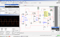
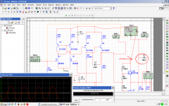
zaec, done, it works 0.000% THD
current trought R2 is abs. same as current trought R5 :O
P.S. ohh its not stable with more gain 🙁( I need more output voltage..
current trought R2 is abs. same as current trought R5 :O
P.S. ohh its not stable with more gain 🙁( I need more output voltage..
Attachments
Last edited:
zaec, done, it works 0.000% THD
current trought R2 is abs. same as current trought R5 :O
P.S. ohh its not stable with more gain 🙁( I need more output voltage..
But it will be a nightmare in the real life due to many reasons. Unstable everywhere. Still very far from a working circuit, unfortunately. I can show many 0.000% THD circuits in Multisim, that will not work at all in real life.
Too many mistakes 🙂
Attached is a working circuit - one of my very old blameless front-ends. It's just upside-down in terms of npn/pnp, comparing to yours.
Note the values. And the way EF ans VAS are arranged.
Explain me what is the diff between your circuit and this -> How to design Discrete Operational Amplifier - Design Guide - Theory - Bart HRK
And also see if the info there is correct 😀
Yours is like mine.. I will use 1k as you and vas stage will be part of the biasing network of the fets ?
Well, both are typical "blameless" topology differential amplifiers.
Mine is improved with the current mirror and emitter follower in front of VAS transistor. It also has got appropriate HF compensation (combination of lag and lead capacitors) for maintaining unconditional stability.
The other one lacks all these things, but has got an emitter follower at the output - makes sense if you need to drive relatively low impedance and/or high capacitance loads.
In the real amplifier, selection of particular transistors for every stage is important. This is not covered by the article.
This topology is rather basic, it's got a lot of areas of potential improvements. As I mentioned earlier, I used this topology long time ago and showed here for educational purposes only.
When designing an amplifier, you should take in account certain requirements you set for yourself. You seem to be too much focused on THD, although there are many other characteristics, even more important - intermodulation distortion, phase response, transients handling, harmonics profile, noise level, slew rate, clipping behaviour, current draw capability and - extremely important - stability in different load conditions.
You can see examples of different approaches, designed with the aim of highly accurate sound reproduction - my recent projects behind the link in the signature below.
By the way, you still did not address the wrong bias of your output stage. It is still around 1mA, which is far below the optimum, resulting in huge crossover distortion. Although it's pretty much corrected by the feedback, it's a bad approach. Much easier - to make each stage as linear as possible, before applying the feedback. If you see what I mean.
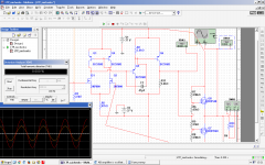
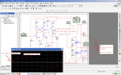
UPDATE: added a 10p shunting cap to the fb solved the oscillation mostly..
maybe if i change the fb resistors, lowering bottom resistor a bit it will be more good more shortcircuiting the HF oscills 🙂
now there is only one problem -> the voltage. Its good but its better to be higher. I havent tested with the LPF cap added..
maybe if i change the fb resistors, lowering bottom resistor a bit it will be more good more shortcircuiting the HF oscills 🙂
now there is only one problem -> the voltage. Its good but its better to be higher. I havent tested with the LPF cap added..
Attachments
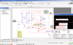
It works vzaichenko, real life works 🙂
I havent tested a OPS yet but with phones it was very clean and nice sound !!!
I was impressed and amazed. There are no clues with it. Just perfect 🙂
With 2n7000 low power mosfets and bc546's the result is same 🙂
Ofcourse I tested on +-12V instead +-37 because MAX Vce and Vds are 60V !!!
I asked for a HV transistors for +-37V and you suggested me BC546 556 for all of my voltages !!!!
No, I did not.................I asked for a HV transistors for +-37V and you suggested me BC546 556 for all of my voltages !!!!
2sc1845 is a nice LTP device.
High Vce0
Your sch are crackpot. No thermal and use aerial instead ! Bonkers.
It works vzaichenko, real life works 🙂
I havent tested a OPS yet but with phones it was very clean and nice sound !!!
I was impressed and amazed. There are no clues with it. Just perfect 🙂
With 2n7000 low power mosfets and bc546's the result is same 🙂
Ofcourse I tested on +-12V instead +-37 because MAX Vce and Vds are 60V !!!
I asked for a HV transistors for +-37V and you suggested me BC546 556 for all of my voltages !!!!
For Q5 - BC556 is not good at +/-37V as it sees the full swing.
It should be at least 2N5401.
The most interesting effects you will see what testing together with OPS.
You don't have equipment to live-measure distortion - you would see substantial numbers (with OPS and the load).
I said to zaichenko not to u 😕No, I did not
Are or Is ? Do you speak english ?Your sch are crackpot. No thermal and use aerial instead ! Bonkers.
In sch is written about thermal feedback and u shouldnt note me about it
I think A1123 and C2631 are better than 2n5401 ?For Q5 - BC556 is not good at +/-37V as it sees the full swing.
It should be at least 2N5401.
Last edited:
You wrote in your schematic
And yes to "Do you speak english?"
And Yes to "are"
all/most of your schematics are bonkers. You don't have much of a clue of how amplifiers are supposed to work.
That "final" schematic is just bonkers.HERE IS NO THERMAL FEEDBACK !!!
JUST RADIO ANTENNA
And yes to "Do you speak english?"
And Yes to "are"
all/most of your schematics are bonkers. You don't have much of a clue of how amplifiers are supposed to work.
Last edited:
BC546/556 will cover all your voltages.
On the other hand, you can cascode the collectors with some high voltage transistors like 2N5551/5401.
I saw how you cascode them but didn't understand how variable resistor(these cascode transistors) lowers the voltage without other resistor to the lower point ??
It must be a voltage divider not only a resistor like two-transinsors setted with a zener.
On another hand if you low down the voltage you must lower it both sides: up and down, not only up ..
And Yes to "are"
all/most of your schematics are bonkers. You don't have much of a clue of how amplifiers are supposed to work.
And Yes to "are" if u have written "schs" instead of sch

I saw how you cascode them but didn't understand how variable resistor(these cascode transistors) lowers the voltage without other resistor to the lower point ??
You just set the voltage reference at the voltage you want and connect the cascode bases to that reference.
It must be a voltage divider not only a resistor like two-transinsors setted with a zener.
Read more about the way zener works. You just set the working current with a resistor - that's it, a simple voltage reference is ready. Don't forget to shunt it with a capacitor for noise reduction.
On another hand if you low down the voltage you must lower it both sides: up and down, not only up ..
Not necessarily - depends on the way your LTP's tail is arranged. In some cases you need to lower the top side only.
You wrote in your schematic
That "final" schematic is just bonkers.
And yes to "Do you speak english?"
And Yes to "are"
all/most of your schematics are bonkers. You don't have much of a clue of how amplifiers are supposed to work.
Still wasting time with this TROLL?
Now claiming he can't test "because he'll wake up Mum and Dad sleeping upstairs" and probably the same who wanted to build an amplifier with one transistor and 2 resistors "because that's all he had available" and thousands others.
Only in DIY Audio 🙄
- Status
- Not open for further replies.
- Home
- Amplifiers
- Solid State
- hv transistors for ltp ??