and whats the diff ? 😀
not works too and theres no difference
Too many mistakes 🙂
Attached is a working circuit - one of my very old blameless front-ends. It's just upside-down in terms of npn/pnp, comparing to yours.
Note the values. And the way EF ans VAS are arranged.
Attachments

Just make R7 = 1.8k, R8 = 47k for your purpose - this particular one was used as a line stage with gain = 2. Just noticed...
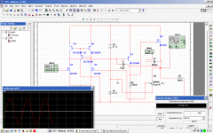
thanks, do you know why a simple phase splitter like this yields such a distortion ?
Single transistor is not that linear device by itself. So, the distortion is THAT LOW because of the deep local feedback, that, however cannot eliminate it completely.
Single transistor is not that linear device by itself. So, the distortion is THAT LOW because of the deep local feedback, that, however cannot eliminate it completely.
Ok, thanks, i planned to do amp with both npn fets at the output stage without any feedback, i think there would be no crossover distortion if fets are same - both n-channels.
Thats why i needed this phase splitter..
P.S. see attachment it didnt worked with quad transistor current mirror :O
Attachments
Last edited:
Hey, I achieved 0.000% with just using a BS170 for the pair.
pair of low power mosfets. same circuit 🙂
added second picture with a fet instead Q6. same performance 0% THD
im confused here what to use 🙄
thinking about a mosfet current mirror too
pair of low power mosfets. same circuit 🙂
added second picture with a fet instead Q6. same performance 0% THD
im confused here what to use 🙄
thinking about a mosfet current mirror too
Attachments

Last edited:
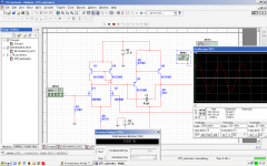
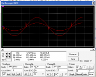
I managed to get it better with 220pf cap but its with a lot of distortion 2%..Another strangines, oscillates when I attached a sample output stage, note that the output stage is for illustrational purposes only . there i sno thermal feedback 🙂
There is no problem with the fb attached locally.
nobody knows ? 😕 
it works on another circuit without current mirror and with pnp pair transistors 😱
it works on another circuit without current mirror and with pnp pair transistors 😱
You seem to be unable to read and copy a sch.
Sort that first and then try to input the correct sch into your simulaton package.
Sort that first and then try to input the correct sch into your simulaton package.

zaichenko,
I managed to do it but why to use pnp with emiter degeneration ?
Actually I like it more, its more beautyful @ the schematic and this is a common sense 😀
I have seen many examples with emiter to rail..
Is it the resistor works as base resistor too ?
Also wondering, I see many examples with the current mirror control to the other side.. How that changes the world ? Global warming ?
I havent tested with an output stage yet, this is with 1MOhm fb pot.
Also wondering is it better to use mos for the input of the opamp or for the output ? All configuration depends on this. I think its for more for the input, for the pair but who am i ? i dont know need test 😀
Also wondering Is it essential to use two stages ?
Also wondering If I have another questions 😀
Attachments
I tested with an output stage and it works only with a cap between last stage of the op amp and the OS (output stage).
resistance to ground of the OS is 200-300k.. I loaded the op amp and min resistance it could handle is 47k, so 200-300 is far far away..
I need it without cap because I need DC offset to control fets more better.
I tested with local fb because simulator gives me convergence issue, ido not know why.
Actually it starts when change the fb but look @ 2nd attach.
P.S. I figured out the power calculation: Max Output voltage ^ 2 / R(load) / 2.64 ( k that i calculated 😀 )
And here it is 36^2/6 / 2.64 = 216/2.64 = 81.9W
This means for 1KW sinus power I need +-127V rails.
This means no transformator at all 😀
Optocouple and go 😀
Touch the cable and vol up the music. Smb tried ? 😀
Attachments

Last edited:
vzaichenko, is your circuit at post #17 your preferred method for biasing the cascode? Do you worry about about zener noise with this arrangement?
An audio amplifier design, whether it uses Mosfets in the output stage or not, is not a simple project for anyone. Most DIYs realize this quite early and learn by building safe, proven designs first. Otherwise they will repair and tinker with working or not-so-working products. Simulation may help you refine a design but I don't know many people who aren't engineers, who can successfully design and develop one without a lot of help over a considerable period of time. It certainly isn't going to happen for you in one thread anyway.
Start with a good book that stretches your learning abilities and find some useful data and guidance about audio amplifier electronics here: https://bgaudioclub.org/uploads/docs/Audio_Power_Amplifier_Design_Handbook_4th_Edition.pdf
Better still, buy the latest edition of the book and pay the author his dues. 😉
Last edited:
vzaichenko, is your circuit at post #17 your preferred method for biasing the cascode? Do you worry about about zener noise with this arrangement?
Post #17 is not my schematic - it's just the one I quickly found on the internet to illustrate what the cascode and emitter follower are in a "blameless" topology.
However, this kind of reference for the cascode - a zener, shunted with a capacitor - is ok. In many cases, you may get more noise from the input pair itself. It can be a concern, if you design a microphone pre-amp, or a phono stage. But in a power amp with 29db gain - no problem.
Thanks vzaichenko. We see buried zeners used as Vrefs in regulators (e.g. the Sulzer and Walt Jung circuits) but the technique seems hardly ever used in power amplifiers published here.
Yes, looking at the latest posts, I've got the same idea as Ian - to recommend some good books on amplifier design and electronics engineering.
Those circuits - although they look like working in a sim - will not work properly in practice for so many reasons that I don't even want to start naming them.
Do you realize, that your output pair is biased to the quiescent current of around 1mA and this causes a huge crossover distortion?
Same with the emitter follower (Q5) - current through R2 is a couple of uA, so its collector current is fully dependent on the base current of Q6, which is not good at all. R2 is so huge value - it does not really influence anything there. Degeneration - another great tool - it's actually a local feedback, increasing linearity and stability and making particular cascade less dependent on active parts' tolerance. But you need to know many other things to really understand why this is the case.
In order to choose the transistors operating points properly, you need to know many things you don't seem to know yet. Take me right - I'm not criticizing, I'm willing to help, but in this case, in order to explain what is wrong, I need to start from very basics and then go through a number of electronics engineering disciplines (normally takes a year or two in the university 😛).
See some electronics theory links on my site here:
My links page
It may look like "too much theory" at a first glance, but it gives you understanding of how transistors work.
And then - just follow Ian's recommendation. Good books and proven designs, until you fully understand them.
Otherwise, it's just playing with the simulator, without any connection to "reality", which is much more "evil", then any simulation (as usual 😀).
Cheers,
Valery
- Status
- Not open for further replies.
- Home
- Amplifiers
- Solid State
- hv transistors for ltp ??