quick question regarding grounding of inputs and outputs. Can i run the ground wire of from board to the input RCA and then on to the output RCA without causing problems. In theory, they are all the same point, but i did not know if there is a more optimal way and if it is possible that some level a signal mixing can occur. The BA3 board does not have enough ground points for the signal grounds of the each of the necessary connections of PSU, input, and output to come back to the board. Also. For the power connection from my PSU to the pre-amp, I am using Speakon 4pin connectors and Mogami quad cable. This allows for a dedicated line for +,-,signal ground, and earth ground. This cable also has a shield that I have connected to earth ground on one end. My question is whether or not this shielding should be left unconnected on the opposite end to avoid ground loop issues.
I am sorry to say I never found a perfect working system, I always had to try....
And over safety ground the wiring of the amp also seems to be important to the system.
Of course I follow some rules.... But not more than you.
Hope you get better answers too .....🙂
And over safety ground the wiring of the amp also seems to be important to the system.
Of course I follow some rules.... But not more than you.
Hope you get better answers too .....🙂
another question. I have all lat fets mounted and boards populated with the exception of the Rs. Will i do harm if i only populate the Rs on the number of fets I would like to try. In other words. If I just wanted to start out with a single pair in order to bias to high level of 1A, wouldn't leaving off the Rs for the other fets just make it look as though they were not even there. Would this harm them? It seems easier to add than desolder an take away.
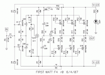
I have come upon a realization in trying to fire up the Lat version. I need a regulator with a lower Vref. Lm431LV should work. I was considering any possibilies of paralleling the the output of the regulator with resistors, but don't think it will work. Oh well. Next time I will know some things better😀
No. The Vgs on the laterals is lower for the current we need. Minimum bias voltage on Lt431 is 5V. With the laterals only takes about 2V to get a full 1A out of each. This is lower than is achievable with that regulator. The regulator I showed has a Vref of 1.25 so using it along with making the top and bottom bias resistors equal, we should be able to get our bias voltage. This almost ensures only using 1-2 pairs based on my heatsink. The only other option is a discrete regulator. Check out the datasheet for the LM431LV and also a great datasheet on biasing mosfets, including the laterals coming your way, AN1645. THis tells you a lot about working through an output stage like we are using, including finding correct resistor values.
isn't it 2V5 ?
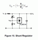
The TL431/TL431Aare three-terminal adjustable regulator
series with a guaranteed thermal stability over applicable
temperature ranges. The output voltage may be set to any
value between VREF (approximately 2.5 volts) and 36 volts
with two external resistors These devices have a typical
dynamic output impedance of 0.2W Active output circuitry
provides a very sharp turn-on characteristic, making these
devices excel lent replacement for zener diodes in many
applications.
TL431 has reference voltage of 2.5. Using the formula that is given by the datasheet, the lowest value you can get is 5V. Split two ways, this is 2.5V for each fet, N & P. This would put the bias of the two laterals at or above 1.5A each. Thats cookin!.
I am using the F4 boards and so trying to make it work with them. The LM431 LV(Low Voltage) has a Vref of 1.25.
buzz
post exact schm you're using and I'll re-draw what's needed
I am using the F4 boards and so trying to make it work with them. The LM431 LV(Low Voltage) has a Vref of 1.25.
ya catchin' my drift ?

now just re-calculate values to have adequate bias range
see - Vo= (1+R1/R2) x Vref ( in datasheet nomenclature )
when R1 is diminishing in value , Vout is approaching Vref value
now just re-calculate values to have adequate bias range
see - Vo= (1+R1/R2) x Vref ( in datasheet nomenclature )
when R1 is diminishing in value , Vout is approaching Vref value
Attachments
Last edited:
.....to doubt you.......
naah ... that's normal
I'm doing that all the time

Last edited:
ok now - let's be serious
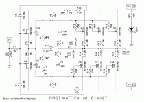
previous schm was drawn just for learning purposes , and now you can see what's changed to have biasing voltage across 431 in range of 4V45 to 5V0
while thinking about needed range , do not forget voltage drop across output source resistors
simple , isn't it .....
previous schm was drawn just for learning purposes , and now you can see what's changed to have biasing voltage across 431 in range of 4V45 to 5V0
while thinking about needed range , do not forget voltage drop across output source resistors
simple , isn't it .....
Attachments
Thanks ZM. I was going to figure up the resistor values today. I don't have 18k and had planned on using another 22K on R9 and keep R8 the same. Only question was to check datasheet and see if current was sufficient for the TL part. Will run the numbers on the different options while traveling today.
ZM,
IN the app note I was telling Generg about, AN1645, they show unequal gate resistors for the two fets. Most schematics I have looked at using these fets show similar resistors, somtimes with caps on as well. I haev read that the caps serve to try to balance the difference in the response of N and P fets. Do the disimilar gate resistors serve a similar purpose or are they different simply because the response of the N vs P fet is different?
IN the app note I was telling Generg about, AN1645, they show unequal gate resistors for the two fets. Most schematics I have looked at using these fets show similar resistors, somtimes with caps on as well. I haev read that the caps serve to try to balance the difference in the response of N and P fets. Do the disimilar gate resistors serve a similar purpose or are they different simply because the response of the N vs P fet is different?
app note AN-1645 , page 10 , first paragraph :
now - just look at mosfet datasheet , first for N polarity , then N polarity ;
observe that both Ciss and xconductance are not identical for both polarities ...
DETERMINING GATE RESISTOR VALUES
The gate resistors, RGN and RGP, are necessary for stability,
MOSFET devices will often oscillate without them. The value
is chosen for best THD performance across the power and
frequency range of operation while maintaining stability. The
values are determined by trial and error adjustment for each
set of devices. In general, the frequency pole location of the
low-pass filter created by the gate resistor and the device input
capacitance, CISS, is chosen to be the near the same for
both the N-channel FET and P-channel FET.
now - just look at mosfet datasheet , first for N polarity , then N polarity ;
observe that both Ciss and xconductance are not identical for both polarities ...
I know their explanation is obvious, but what is not so obvious is how most output stages containing complimentary fets have the same value for gate resistors. If it is optimal to have different values for each fet, then why doesn't the F4, F5 and other complimentary topologies have disimlar values. The fet characterisitcs are disimilar in those as well. Is this quibbling over spilled milk or is it an important thing to do. I remember in thread about F4, where you made the comment that the dissimilarity of the output fets was in fact part of what contributed to the final sound. Would not the same be true for these fets as well? Ihave a Tek 465B sitting on the shelf but I am new to it as with all these things.
- Status
- Not open for further replies.
- Home
- Amplifiers
- Pass Labs
- Humble Beginnings:D