The next step
It still could be U1 or U2, or maybe R30 was really set way, way off, over 1,800 seems a bit towards the end of its travel - it looks like it was set by a monkey using a fork for a tool. When I get the new pot put in, and take the next the reading, I will then see what kind of waveforms I have and then check some DC voltages at the test points.
Hopefully, I can finish this part tonight, the 1468 is installed and I just found my bag of 2K 10 turn pots, so after dinner it should get done.
Thanks guys,
Steven
Well rather than check the DC voltages, I decided to pull U1 and R30, replacing U1 with a nice machined socket and an LT1468CN8, 1609 datecode and I removed pin 8, and R30 (which I measured to be set at 1,814 ohms) and maybe later replace two of the 1000/35 volt lyrics in the power supply. I will set the new 10 turn pot at 1000 ohms (centered) and see if I self measure better than the 11% +/- distortion reading I had before. If it is suddenly way under 1%, or under 0.1% then it was either a bad solder joint, a HA2625 IC defect, or a bad setting of R30.The oscillator is not stabilizing for some reason. Check the TP for Jfet gate, what dc voltage do you have there?
It would be more telling to use dc coupling for now.
It still could be U1 or U2, or maybe R30 was really set way, way off, over 1,800 seems a bit towards the end of its travel - it looks like it was set by a monkey using a fork for a tool. When I get the new pot put in, and take the next the reading, I will then see what kind of waveforms I have and then check some DC voltages at the test points.
Hopefully, I can finish this part tonight, the 1468 is installed and I just found my bag of 2K 10 turn pots, so after dinner it should get done.
Thanks guys,
Steven
The 1468 is installed, 2K 10 turn pot is in, two new caps in the Analyzer section of the power supply (1000/35v) are installed...
Not quite the results I was hoping for
Selftest = 13.5% distortion!
I turned the pot up (counter clockwise in this case) a few turns, maybe it is not quite as high as 1,814 here, but the distortion went down to 11%, so back to where we were before, more or less.
Powered on a Fluke meter.
PS +15.18 / -15.32 v.
TP1. +0.587 v.
TP3 +13.86 v.
TP4. +12.03 v.
TP5. -12.88 v.
TP6. +1.087 v.
TP8. +1.667 v.
Looking like the Fet or U2 ?
Any insight? Thanks guys,
Steven
U2
PIN
12 +13.86 v.
13 +13.87 v.
14. +12.02 v.
Steven
Voltage on TP8 is too high. should be less than 1Vdc. There is way too much offset on TP1. U2 doesn't matter at this point. Your problem is with the oscillator or control. Show the wave form on TP1 again. Is it still clipped.
Short TP8 to ground and see if the oscillator stops.
Short TP8 to ground and see if the oscillator stops.
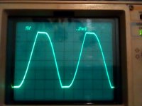
It is almost 30 vp-p!
Here is current TP1 still clipped.
Then TP8 shorted to the Gnd pin. No change it doesn't stop!
-Steven
Here is current TP1 still clipped.
Then TP8 shorted to the Gnd pin. No change it doesn't stop!
-Steven
Attachments
Last edited:
Before I noticed that U1 (on the 1468) pin #5 was not in the socket, bent under, I pulled the IC and corrected that, still no change, voltages remained the same on all test points.. and on U2 Does that help at all?
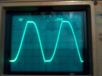
Again, here is current TP1. Then TP8 shorted to Gnd. 28v p-p. Much more than the signal (20vp-p) is on the schematic in the manual.
I am thinking there is a resistor that is open, and the gain is too high on U1.
-Steven
Again, here is current TP1. Then TP8 shorted to Gnd. 28v p-p. Much more than the signal (20vp-p) is on the schematic in the manual.
I am thinking there is a resistor that is open, and the gain is too high on U1.
-Steven
Attachments


It appears that Q2 may be open. The reported gate voltage (TP6) should turn the FET to low resistance, but seemingly doesn't because the oscillator hasn't stopped. The gate voltage is also oddly high. I would expect the gate-channel junction to forward bias at around 0.7V, so this is also suggestive of a defective FET. (By way of confirming proper proper U2, if TP5 and TP6 voltages remain as reported, U2 pin 8 should be around +8V. It would be good to confirm all is well with U2.)
Back to confirming suspected Q2 failure: Adjust R30 to maximum resistance, as this is least challenging for Q2 on-state resistance. Then try shorting the R52-C30-Q2 (i.e. across FET) node to ground. If the oscillator stops, the implication is an open Q2.
If this test does not stop the oscillator, first order of business is to find out why it doesn't. If you arrive at this unhappy spot, perhaps you could show a new picture of TP8 with DC coupling.
Good luck!
Followup speculation: a shorted gate-channel Q2 failure would also explain the slightly elevated TP1 bias voltage David noted in his post.
Just a thought. At this high an output Vpp, it may too strong to shut the oscillator down by forcing the jfet to low Z If my State variable goes to clipping there is no hope in shutting it down. Must power down then restart.
Although I would expect at least some reduction of Vpp. A bit less clipped.
Although I would expect at least some reduction of Vpp. A bit less clipped.
Last edited:
Hi David,
I hope shorting across Q2 quenches oscillation, but I've been surprised many times by the unexpected.
I don't know what of make of your experience with your SV oscillator. At what frequency does this happen? Any evidence that slew rate limits are in play? I'm always interested in learning from other designs, if you care to divulge your schematic. 😉
We could continue in different thread if you think this drifting too far off topic.
You can read the entire development of my SV oscillator in the Low distortion oscillator thread.
Fortunately it's all covered in the first half of the thread. The process of all the 339A mods are in there too. These were started by me and Richard Marsh took over later on. Spike consolidated the mods in a DIY wiki.
Hi, Well I removed Q2 from the set I am working on, and also from the other 339a, the one with two broken switch wafers. This Q2 when put in one of those fancy testers, with multiple line and graphic readouts, and it did not even register as a J-fet. It was a diode, so, yes, I said a resistor was open and that the U1 output was way too high clipped at 28 v p-p, instead of 20 v p-p., well Q2 was the resistor which was open.It appears that Q2 may be open. <snip>
Interesting, as an aside, with the made-in September, 2016 LT1468CN8 in place, the clipping on the distorted waveform did seem more symmetrical, than with the 1983 HA2625 part (I think that was U1's designation or equivalent). In light of this failure, the other Q2 part, which measured as a 5.3 mA at 3.7 volts J-fet, those readings seem like an OK value, as the only numbers for the VCR2N part imply a rating of 15 volts and 10 mA.
The Q2 Fet seems usually has about 7.5 volts on it, which brings up the question does it fail often, and would a more modern and higher voltage part be more linear and/or more reliable? I don't have a good selection of J-fets, so really have no way to test other parts. I do have a 2SJ211 J-fet that I took off a Sencore board, there were also three MPF960's, but they are not Jfets according to the tester, I wonder if an N-MOS part would be better or worse?
Has anyone ever experimented with other parts for Q2? It is something to think about!
So on Saturday, I will try the other Q2 part and see if it works well, and hopefully the new U1 output will have less than normal distortion once the level is adjusted to +/-10 volts p-p. Where it should be. The replacement pot I installed for R30, I forget if it is a 10 turn or a 25 turn trimpot, I did not have the bag marked, maybe I can look up when I ordered them must be about a year ago, when I ordered the LT1468's.
Looking forward to seeing the meter reading down in the -90dB /-100dB range, after all this work, and learning 😱.
Steven
Hi Steven,
Seems like you're making good progress.
I have no personal experience with other J-FETs, but I bet other forum members will have suggestions, as I know suitable substitutions have been found. The FET Victor uses in his design would be a good candidate.
The "Amplitude Adjust" annotation HP has next to R30 is a bit misleading. It allows the Q2 gate voltage to be adjusted to a "sweet spot", -0.4V if memory serves, and spelled out in the adjustment section of the manual. Once the control loop is working properly, actual p-p output is controlled by U2A, R34, R35, and the +15 rail, in concert with the fact that TP4 must be 0VDC when the loop has settled.
Good luck!
Last edited:
The Jfet in the 339A is a selected part by HP as most of the active parts are. I have used the 2N4391 or 2N4392 with varying results. But one of these should be able to meet spec. I did get the original non selected part from Electronic Goldmine. But that was years ago. It's been 7 - 8 years since I did all this and would it take a bit of digging to find the original part number.
Edit: VCR2N Vishay Siliconix
Edit: VCR2N Vishay Siliconix
Last edited:
I went through the low distortion oscillator thread. I't looks like the work on the 339A starts near post 2262. This can save you much reading.
Thanks, David.
I started at the beginning. It's kind of like starting a lengthy novel (I'm thinking Crime and Punishment)--- a long slog, but enjoyable and rewarding. 🙂
I started at the beginning. It's kind of like starting a lengthy novel (I'm thinking Crime and Punishment)--- a long slog, but enjoyable and rewarding. 🙂
Last edited:
When I went in today I broke up a socket and installed pins for placing the other Q2, after three hours of fighting the switch cross couplers and wiring, I even tried using long needle nose pliers, to try and install the used part with barely 1/4 inch leads, and I gave up...Hi Steven,
Seems like you're making good progress.
I have no personal experience with other J-FETs, but I bet other forum members will have suggestions, as I know suitable substitutions have been found. The FET Victor uses in his design would be a good candidate.
The "Amplitude Adjust" annotation HP has next to R30 is a bit misleading. It allows the Q2 gate voltage to be adjusted to a "sweet spot", -0.4V if memory serves, and spelled out in the adjustment section of the manual. Once the control loop is working properly, actual p-p output is controlled by U2A, R34, R35, and the +15 rail, in concert with the fact that TP4 must be 0VDC when the loop has settled.
Good luck!
I removed the socket pins and finally got the part in, taking a few minutes. Pins might be fine when your part has full length leads, but not when they are twice the thickness of the PC board, and so many parts and wire bundles impede your way.
OK, about that "sweet spot" I did not initially notice the "minus" sign. At first I was getting pretty good readings with about -3.66 volts at TP8, and turned it up until I was at +0.4, readings were still OK, but tomorrow I will adjust it downward to -0.4 volts at TP8.
Set at present gives the following readings:
PS. +15.13 /-15.19 Volts
TP1 -18.7 mV. Sine output is 6.72 v AC (a bit low, should be 20v p-p. or about 7.07 v AC)
TP3 8.99 V.
TP4. 3.3 mV.
TP5. -8.07 V.
TP6 0.1 mV.
TP8. 0.408 V.
THD -91.0 dB filters out
-93.5 dB w/80 kHz. Filter in.
I seem to recall best calibration involves two trimpots, R30 and another one, was that the one where four at grouped together, which one upper left hand corner? Since I made R30 a 25 pin part, maybe I can do the same on the other one before the final adjusting.
Steven
The second pot is for adjusting the feedback ratio to the gate of the Jfet. If you are referring to the mods.
Perhaps distortion will improve once TP8 is readjusted. TP4 and TP3 look about perfect so I don't know what to make of the TP1 ac amplitude. Unless ripple at TP3 is abnormally large, all looks nominal. I'll try to scrutinize spec later.
TP5 looks very odd, but that may be function of +0.4V at TP8. When TP8 set to -0.4V, expected TP5 would be about +0.8V.
Good luck!
Followup:
See section 4.18 of manual. The manual specs 3V rms into a 600 ohm which means 6V rms open circuit. I think your observed output level of 6.7V rms is fine.
To elaborate a bit about TP5: with at +0.4V on TP8, the expected TP5 voltage would be -0.8V but you report -8.07V. This leads me to suspect the Q2 gate-channel junction is clamping TP8. I imagine all will be ok when TP8 is readjusted to nominal.
- Home
- Design & Build
- Equipment & Tools
- HP339A distortion analyser