I am doing some time-passing activity but am a little ambiguous about my procedure.
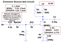
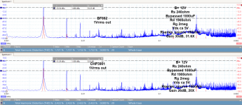
Here I am comparing BF862 and CPH3910, and I have set them up in exact same circuits, with same value components. But this means one device idles at a slight different Id and they also have different gains... Should I adjust values for same Id? Should I adjust values for same gain? If adjusting for same gain, do I add source degeneration, or alter the load on the drain?
I am thinking I can adjust the source resistor for nearly same Id. Then I can AC-couple an amount of source resistance and adjust until the gain is similar for all devices under test.
Or are my values close enough and a few tens of mA wont make a big enough difference anyways?
My intent is to compare and measure gain, distortions, noise, Cin... what else should I add?
For noise tests I intend to simply add series resistance on the input until noise floor rises by 3dB. This is accurate enough? I will be using a 10x and 100x LNA between JFET and analyzer.
Here are some pictures of the circuit and some measurements. I dont know if I ever actually get something sensible out of this.
Oh, I misspelled CPH3910 in many screenshots...
Attachments
-
 testcircuit.png130 KB · Views: 161
 -
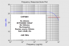 CHP3910_commonsource_RsBypassed.png48.7 KB · Views: 78
 -
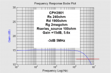 CHP3910_commonsource.png51.7 KB · Views: 69
 -
 bf862_commonsource_RsBypassed.png48.6 KB · Views: 79
 -
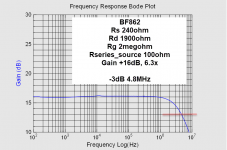 bf862_commonsource.png55.9 KB · Views: 70
 -
 BF_CPH_degen_1Vrms_thd.png430.4 KB · Views: 132
 -
 BF_CPH_2Vrms_thd.png409.2 KB · Views: 129
 -
 BF_CPH_1Vrms_thd.png428.9 KB · Views: 132
 -
 BF_CPH_comparingdata.png247.2 KB · Views: 151
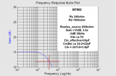
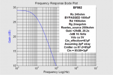
Just adding the shots of my trying to measure input capacitance. I add 200kohms in series with signal gen. This in parallel with the 2megohm gate bleed gives a source impedance of 182kohms.
I then find the C required for the given -3dB cut-off.
I assume 2pF stray cap on the circuit input so subtract 2pF from the calculations.
Comments on this method?
Should I consider the response when using 100ohm as source resistance? (shown in above post)
Edit: I divide by gain to eliminate miller
I then find the C required for the given -3dB cut-off.
I assume 2pF stray cap on the circuit input so subtract 2pF from the calculations.
Comments on this method?
Should I consider the response when using 100ohm as source resistance? (shown in above post)
Edit: I divide by gain to eliminate miller
Attachments


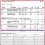
Anyone know what Onsemi means with noisefigure without stating what impedances or noise levels they refer to? I mean, for noise figure, don't you need the input thermal noise as reference? Any measure given in dB should have what the reference is, no?
Its meaningless without that information, yes, so perhaps they are quoting the absolute best noise figure for any situation though (typically of the marketing-blurb parts of datasheets)Anyone know what Onsemi means with noisefigure without stating what impedances or noise levels they refer to?