I'm using a resistor (110R) to set the bais for my single pair of lateral FETS (2sk1058/j162). The vas (mje340) is supplied by a ccs of around 11.6mA. How do i calculate the value for the ac bypass cap across the 110R bais resistor?
What works in practice is C=(2 x PI x R x F)^-1 where F is the lowest frequency you want to pass, example 20Hz. For R = 110 Ohm it is 72.3 uF, next size up is 80uF.
wow, i was going to try 0.1 to 2.2uF, as this is what i have seen on circuits that used a Vbe multiplier transistor. Thanks for the info.
Nico, That's the formula for an RC filter. In this case we are talking about a resistor in parallel with a cap.
I would look at this like a shelving filter - the R//C into the load represented by the Gate of the driven mosfet in parallel with the impedance to the rails. The Gate impedance is likely very high, so almost any capacitor will do to bypass a 110R resistor and not significantly impact the HF response. We use 100-200R as gate stoppers, right?
Practically, a few uf should be fine - 1uf film and/or a small electrolytic. 100 uf wouldn't hurt, but would possibly create a delay starting the mosfets with time constant set by the resistors feeding it. A couple uf would take a lot less time to charge up.
Disclaimer - I am not an electrical engineer, I would like to go through Bob Cordell's book but don't have it yet.
wow, i was going to try 0.1 to 2.2uF, as this is what i have seen on circuits that used a Vbe multiplier transistor. Thanks for the info.
The formula given is correct although I am not convinced you need a capacitor at all. After all the voltage across the bias should really be constant. If its not then you need a Vbe multiplier otherwise you might start cooking or under biasing the MOSFETs.
I am not convinced you need a capacitor at all. After all the voltage across the bias should really be constant.
The theory is that one fet is fed the signal directly, the other thru the bias R, so the cap is to ensure both fets see the same signal. Bias voltage variation is not the issue here.
please post your schematic
Depending upon the rest of your topology, the effects of the cap range from almost non-existent to perhaps medium significance. I'm imagining more facts than are currently in evidence...so I'll state my assumption.
Cdom wraps around the Vas transistor, to the low side of the 110 Ohm resistor. That defines the forward gain of the VAS to the low side of the 110 Ohms. If the Vas has a small emitter resistor, say 10 Ohms or less, the Vas will have a high frequency output impedance of about 10 Ohms. That says the bottom FET is driven by 10 Ohms, and the top FET sees 120 Ohms at high frequencies. Whether this matters depends upon the capacitive loading seen, and the bandwidth of your amp. Capacitive load depends on the output fets, and whether they have emitter follower drivers...
The main reason to include such a cap is to make the high frequency characteristics of the amp more similar between the push and pull sides.
Thanks for your reply, djoffe.
My bmp file is 800k, cant upload now.... (not sure how to reduce it!)
Basically the amp is a 3 stager, pnp ltp input, a single bjt CE mode vas, with the fets driven directly from the vas collector.
The vas is supplied from a CCS.
The Vas emmiter resistor is 39R
The bandwidth is 50KHz
There is no miller cap, instead a r-c lag network is used instead.
don't save it as bmp.Thanks for your reply, djoffe.
My bmp file is 800k, cant upload now.... (not sure how to reduce it!)
Use one of the compressed file formats.
png, gif, etc. Find the one that creates the smallest file and is still legible.
Different pics work with different pic formats. Some work with colour but badly (big) with black and white, some deal with lines well, others deal with photos well.
Then compress the file using software, Irfanview works well and is cheap.
dropping bmp size
Here's a way that's probably on your computer. Open the bmp in paint.
Assuming you're on microsoft, START=>All Programs=>Accessories=> Paint.
When in paint, File=>Open=>yourfile.bmp. Then File=>Save As, and in the Filename Box, change the filename to yourfile.png, and click save.
That's it...
Here's a way that's probably on your computer. Open the bmp in paint.
Assuming you're on microsoft, START=>All Programs=>Accessories=> Paint.
When in paint, File=>Open=>yourfile.bmp. Then File=>Save As, and in the Filename Box, change the filename to yourfile.png, and click save.
That's it...

Henry8,
Your circuit will work fine, you do not need the zener and diode protection on K1058/J162 they are built into the devices.
With 55V rails you will achieve around 120 watt into 8 ohms. If you use a separate low current supply of 10 or so volt higher on the pre-output stage than that of supplying the output devices you will swing close to the output rails as well as reduce distortion.
Nico
Henry8,
Also try a bootstrap in place of the constant current source. Some folk enjoy the warmer sound of a bootstrap which has higher 2nd harmonic, while others prefer the more "clinical" sound using a CCS which has higher 3rd harmonic.
Also try a bootstrap in place of the constant current source. Some folk enjoy the warmer sound of a bootstrap which has higher 2nd harmonic, while others prefer the more "clinical" sound using a CCS which has higher 3rd harmonic.
One final comment is that you can replace V2 with two forward biased diodes that will bias the output devices at about 270 mA without the need of adjustment. 1N400X is quite sufficient for the purpose. You do not have to by-pass the diodes with a cap.
An absolute final comment is to decouple your signal and feedback ground from the power ground with a 10 ohm resistor bypassed with 100 nF cap to avoid ground loops.
Henry8,
There is an interesting trick of the trade that you may want to experiment with, that is of placing a cap of around 10 -22 uF cap between the emitters of the differential amp when using degeneration resistors. It places the emitters at the same AC voltage and therefore the AC summing point is at the emitters and not the junction the degeneration resistors and results in a reduction the THD.
That is me for tonight, cheers
Nico
Henry8,
There is an interesting trick of the trade that you may want to experiment with, that is of placing a cap of around 10 -22 uF cap between the emitters of the differential amp when using degeneration resistors. It places the emitters at the same AC voltage and therefore the AC summing point is at the emitters and not the junction the degeneration resistors and results in a reduction the THD.
That is me for tonight, cheers
Nico
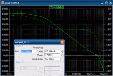
That will work some of the time on some amps. On the typical "blameless" , watch out .... even a 4.7uF across LTP emitters will put your unity gain point well beyond where you have a safe phase margin (oscillation - example below). Be careful !! I found that it DOES work well on a design that has no current mirror (i.e lower OL gain).
OS
Attachments

- Status
- Not open for further replies.
- Home
- Amplifiers
- Solid State
- How to calculate bypass cap across bias resistor?