
Meant to say "from one side of the module to the other side without going to the load." Poorly worded.Cross conduction is current flowing from one side of the module that doesn't go to the load. At least that's what I call it, maybe there's a better term.
Normally, we want to have each section use their own coupling caps so that there is no coupling at DC between sections.
Could you expand on this more?
I’m assuming coupling capacitors 100uF should not allow DC coming from U1 outputs to be present at LM3886 inv and non-inv inputs.
Or what you are saying is that there can be a possibility where different voltage will be present at LM3886’s inv/non-inv corresponding inputs?
Should 1K+1K resistors prevent large current from developing between those corresponding inputs?
A servo (one per section) might be a better solution as the capacitors are smaller and can be precision type and tolerance, which avoids fighting conditions at near DC frequencies where cap tolerances will cause different output voltages leading to cross currents.
I don’t know how to implement servo for the difference amp topology.
Last edited:
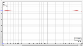
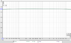
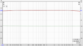
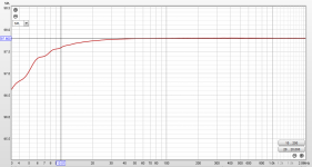
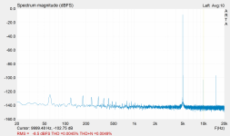
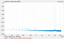
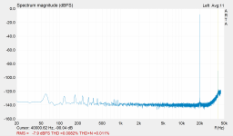
This is somewhat normal because in the case of a higher offset, the current that constantly circulates between the amplifiers creates a kind of class A at low power.Here are attached measurements results for both channels.
Interestingly, the channel that is closer to the psu has offsets of -7.9mV and 6.4mV (-0.8mV) but shows less THD figures.
More measurements are attached:
Attachments
-
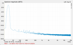 channel1-smaller offset - 30hz.PNG456.3 KB · Views: 75
 -
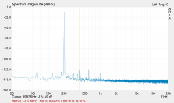 channel1-smaller offset - 200hz.PNG446.7 KB · Views: 81
 -
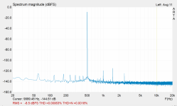 channel1-smaller offset - 500hz.PNG445.7 KB · Views: 69
 -
 channel1-smaller offset - 1000hz - cursor2.PNG284.1 KB · Views: 80
 -
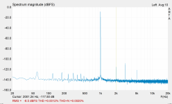 channel1-smaller offset - 1000hz.PNG383.3 KB · Views: 69
 -
 channel1-smaller offset - 5000hz.PNG267.8 KB · Views: 72
 -
 channel1-smaller offset - 10000hz.PNG395.4 KB · Views: 63
 -
 channel1-smaller offset - 20000hz.PNG453 KB · Views: 82
Hi gooduser,
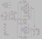
If you still wish to explore a DC servo, I've attached the PDF below for your consideration.
The drawing is very abbreviated, but with enough detail to convey concept, I hope. Not shown but implied is elimination of C7 and C8. Also not shown are supply bypass caps, compensation caps on the LM3886, etc.
Briefly, the servo amp is a differential integrator (Ca, Cb, Ra, Rb) with offset correction applied to the lower power amp via Rc. If just a single amp was being servo nulled, Ra would be grounded; instead it connects to the other amp, which acts as the nulling reference voltage. (Rd through Rf are added to maintain matching for common-mode rejection.) Another detail not shown is offset trimming for the OPA134. This opamp features offset nulling which should be incorporated; data sheet specifies 2mV offset, but adding the pot will enable trim to null.
Attachments
I've made an embarrassing oversight in my servo suggestion. I was so focused on the differential integrator that I failed to notice that though it nulls the difference between the two power amps, it doesn't null the amps to 0V offset re ground. So I've made an addition to my original sketch. The added opamp nulls the upper LM3886 to 0V offset, while the other continues to nulls the lower amp to 0V difference.
The newly added opamp should inherently null the upper power amp offset to less than 2mV, but I've added offset to support trim to 0V; the pot should provide about +/-5mV trim range. I note that it requires fewer parts to apply the upper design to both power stages and abandon my original differential integrator. You can then use the dual OPA2124 if you wish to simplify layout.
I hope this text is decipherable and I'm sorry to have led you in a messy direction.
Attachments
I've made an embarrassing oversight in my servo suggestion. I was so focused on the differential integrator that I failed to notice that though it nulls the difference between the two power amps, it doesn't null the amps to 0V offset re ground. So I've made an addition to my original sketch. The added opamp nulls the upper LM3886 to 0V offset, while the other continues to nulls the lower amp to 0V difference.
I was thinking about this just this AM while walking. While it's probably OK to just null the difference (it's not very big after all), it's better to null both channels to 0 V. But if you need 2 op amps anyway why not just null both circuits to 0 V with identical circuits? I get a little suspicious of one loop chasing another.
Plus if you null both channels directly to 0 V, you could remove the blocking cap at the bottom of the divider that gives you unity gain at DC - assuming that your nulling circuit has enough range to handle worst case offset times gain which it probably does.
The other thing you could do with nulling circuits on both sides is add a window comparator so that if a big DC offset occurs due to a fault you could trip some kind of speaker disconnect or shutdown.
Few questions:Hi gooduser,
If you still wish to explore a DC servo, I've attached the PDF below for your consideration.
The drawing is very abbreviated, but with enough detail to convey concept, I hope. Not shown but implied is elimination of C7 and C8. Also not shown are supply bypass caps, compensation caps on the LM3886, etc.
Briefly, the servo amp is a differential integrator (Ca, Cb, Ra, Rb) with offset correction applied to the lower power amp via Rc. If just a single amp was being servo nulled, Ra would be grounded; instead it connects to the other amp, which acts as the nulling reference voltage. (Rd through Rf are added to maintain matching for common-mode rejection.) Another detail not shown is offset trimming for the OPA134. This opamp features offset nulling which should be incorporated; data sheet specifies 2mV offset, but adding the pot will enable trim to null.
- can TL052 be used instead of opa134?
- are zener diodes providing 12V?
- how would I go about offset nulling for opa134? Is adding trim pot to Ra or Rb will do the trick? Or Rc?
I've made an embarrassing oversight in my servo suggestion. I was so focused on the differential integrator that I failed to notice that though it nulls the difference between the two power amps, it doesn't null the amps to 0V offset re ground. So I've made an addition to my original sketch. The added opamp nulls the upper LM3886 to 0V offset, while the other continues to nulls the lower amp to 0V difference.
Will this mean that if differentiator schematics (first variant) is used the offset to the GND will be whatever offset is on the top LM3886? Top LM3886 is used as a reference, right?
If top LM3886’s offset is 10mV then the second the second LM3886 will be fed corresponding voltage to create same 10mV offset at its output?
Will this mean the amp will operate more towards class A?
Not shown but implied is elimination of C7 and C8. Also not shown are supply bypass caps, compensation caps on the LM3886, etc.
I was thinking to move DC blocking capacitors in front of the first stage of the instrumentation amp, in my case U1, LM4562. They could be 2.2uF film type and work with 47k resistors to create high pass filters for in+ and in- signals. And I think I need to closely match those together.
In that way amp will be protected from the faulty equipment plugged into its inputs. Just in case DC will be out of the range of servo adjustment.
TL052 should work equally well. I suggested the OPA134 as Bob Cordell used that series in his revamp of Haffler amps.Few questions:
- can TL052 be used instead of opa134?
- are zener diodes providing 12V?
- how would I go about offset nulling for opa134? Is adding trim pot to Ra or Rb will do the trick? Or Rc?
The 12V Zeners ware part of input protection for the opamp. If you adopt the revised servo to null each power amp, simplified protection and elimination of one 1uF cap are part of parts savings.
Nulling of OPA134 is shown in Figure 29 of TI data sheet. Simply adding resistance doesn't correct opamp offset error.
40 years ago, I used to make a lot of great plans like these. But that was before SPICE, especially free LTC spice. I have avoided more than one whoops oversight by simulating things before I suggest them. And posting a SPICE schematic makes a nicer drawing.I've made an embarrassing oversight in my servo suggestion. I was so focused on the differential integrator that I failed to notice that though it nulls the difference between the two power amps, it doesn't null the amps to 0V offset re ground. So I've made an addition to my original sketch. The added opamp nulls the upper LM3886 to 0V offset, while the other continues to nulls the lower amp to 0V difference.
The newly added opamp should inherently null the upper power amp offset to less than 2mV, but I've added offset to support trim to 0V; the pot should provide about +/-5mV trim range. I note that it requires fewer parts to apply the upper design to both power stages and abandon my original differential integrator. You can then use the dual OPA2124 if you wish to simplify layout.
I hope this text is decipherable and I'm sorry to have led you in a messy direction.
Unfortunately I’m running behind on simulating both of those circuits. I’m just curious how they will run. But have to take care of other responsibilities for now… 🤷🏻♂️
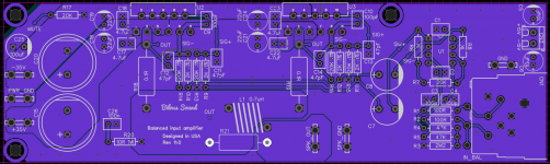
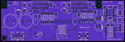
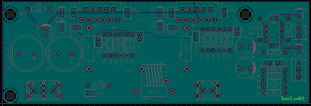
Updated layout for the PCB and fixed some major mistakes in the schematics.
Instead of using just single capacitor in the feedback loop, it is now fixed with adding resistor in series just like datasheet has it. Another fix was gain structure - now LM3886 has gain of 2 x 10 and first stage has gain of 1.1.
Also, attached is the gerber file for anyone who wants to repeat the project.
Attachments

- Home
- Amplifiers
- Chip Amps
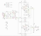
- How bad input voltage offset difference between the two LM3886 will be in the schematics below?