HV-Amp II
Hi again,
second part of the amp.
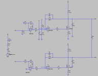
The input signal is fed to the noninverting input of the OPamp (3), a 2 stage design consisting of the transistors M1..5 and M21, M22 (M3..15 form a biasing network). The negative input will be connected to a feedback network. The output voltage (M22) drives the Gate of the inverter stage, consisting of XMH1, 112, RT1, 2, CT1, 2 and zener diode D2.
The CCCS is made up of XMH5, 6, RT5...8, and CT5, 6.
Both stages drive the sourfefollower consisting of XMH3, 4, RT3, 4, CT3,4 and zener diode D3.
Zener diode D1 dicharges the load capacitance when output signal drops.
The specialty is the use of cascaded MOSFets (depletion) throughout the 3 high-voltage stages and the accompanying RC-biasing networks.
Function:
With 0V at the NI-input and output of the OPamp (M22) the inverter tansistors XMH1 and 2 are open, the CCCS transistors XMH5 and 6 are shut.
A positive going signal at INP opens up M22 and shuts down XMH1, 2. The CCCS now supplies the current to charge the input capavitances for the transistors. The voltage level at point 7 rises and opens up XMH3, 4 of the sourcefollower. So does the voltage at the ouput of the circuit, thereby charging up the connected load capacitance. A external feedback network connected between the output and the INN input controls the amplification level.
When the input signal is falling the whole circuit works similar as to the positive going signal, but with diode D1 helping to discharge the load capacitance. The inverter opens up and the sourcefollower shuts down.
The use of RC-Biasing networks shall ensure equal voltage distribution at the gates of the transistors with fast transients regardless of tolerances within the biasing resistors and input capacitances of the gates.
jauu
Calvin
Hi again,
second part of the amp.
The input signal is fed to the noninverting input of the OPamp (3), a 2 stage design consisting of the transistors M1..5 and M21, M22 (M3..15 form a biasing network). The negative input will be connected to a feedback network. The output voltage (M22) drives the Gate of the inverter stage, consisting of XMH1, 112, RT1, 2, CT1, 2 and zener diode D2.
The CCCS is made up of XMH5, 6, RT5...8, and CT5, 6.
Both stages drive the sourfefollower consisting of XMH3, 4, RT3, 4, CT3,4 and zener diode D3.
Zener diode D1 dicharges the load capacitance when output signal drops.
The specialty is the use of cascaded MOSFets (depletion) throughout the 3 high-voltage stages and the accompanying RC-biasing networks.
Function:
With 0V at the NI-input and output of the OPamp (M22) the inverter tansistors XMH1 and 2 are open, the CCCS transistors XMH5 and 6 are shut.
A positive going signal at INP opens up M22 and shuts down XMH1, 2. The CCCS now supplies the current to charge the input capavitances for the transistors. The voltage level at point 7 rises and opens up XMH3, 4 of the sourcefollower. So does the voltage at the ouput of the circuit, thereby charging up the connected load capacitance. A external feedback network connected between the output and the INN input controls the amplification level.
When the input signal is falling the whole circuit works similar as to the positive going signal, but with diode D1 helping to discharge the load capacitance. The inverter opens up and the sourcefollower shuts down.
The use of RC-Biasing networks shall ensure equal voltage distribution at the gates of the transistors with fast transients regardless of tolerances within the biasing resistors and input capacitances of the gates.
jauu
Calvin
Attachments
Yes , it works , but for now , i can only measure , but not listen , as ESL panels are waiting to be built , too 🙂.
Regards,
Lukas.
Regards,
Lukas.
Hi,
Finally , i set up my amp with esl to listen.The panel is 50x12.5 cm , 1.5 mm spacers , 3.8mm diapraghm , coated with thin layer of shoe polish.It fully charges in about 10-30 seconds.
EHT supply is approx 2.5 kV.
Amp's power supply is ~ 650V.That gives around 450Vrms at output.
In no way is it quet ! Panel's resonance is a bit too low , so it touches stators at full volume.Cutting out low frequencies with equaliser greatly improves maximum SPL.
However , the sound is a bit noisy, especially high frerquencies.
It seems that noise comes from panel , and not amplifier , but will have to check this out.
Anyway , its amazing to see such a thing producing sound !
regards,
Lukas.
Did you measure the amplifiers output? The 13k resistor and the panel work together like a lowpass filter, this could cause distortion at high frequencies.
Hi,
Output at 20 khz is less that 1 db down.
In this design , resistor limits full power bandwidth.At 200 pF load , it is approx 20kHz.
I was also thinking that internal mosfet's diode may open due to EHT supply leakage.EHT voltage is negative in respect to ground.
I will try to do some measurements when i get stators powder coated.
Regards,
Lukas.
bigwill said:Would you say this design would be difficult to build for a newbie?
It's not that hard to build, just be very very carefull with the high voltage power supply.
ALso you need a polarizing supply just like when using a transformer.
Hi,
Really , it is not very hard to build.Still , the design is not finished yet.
While i havent got it working well , i cannot recommend to anybody.
Also , the high voltage middle point is grounded.So , protective grilles are required , so nobody can touch even one of stators.
Regards,
Lukas.
Really , it is not very hard to build.Still , the design is not finished yet.
While i havent got it working well , i cannot recommend to anybody.
Also , the high voltage middle point is grounded.So , protective grilles are required , so nobody can touch even one of stators.
Regards,
Lukas.
Hi,
Finally , i have made some measurements of the amp.
In simulations , everything worked perfect , with distortion levels <-80db between 20 - 10 000 Hz , at full output swings.
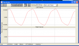
But , when measured , i get very high distortion(1%-15%) at low frequencies.Can this be "motorboating" ?
The most distortion comes in range of 20-200 Hz.
Also , rising output level greatly increases THD.
Regards,
Lukas.
Finally , i have made some measurements of the amp.
In simulations , everything worked perfect , with distortion levels <-80db between 20 - 10 000 Hz , at full output swings.
But , when measured , i get very high distortion(1%-15%) at low frequencies.Can this be "motorboating" ?
The most distortion comes in range of 20-200 Hz.
Also , rising output level greatly increases THD.
Regards,
Lukas.
Is that the output of the two amps together working as a bridge or is it just one amp?
The dc offset might be wrong, causing one amp to clip before the other, this causes the gain to be cut in half, showing this kind of distortion.
The dc offset might be wrong, causing one amp to clip before the other, this causes the gain to be cut in half, showing this kind of distortion.
Hi,
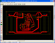
I measured with both amps connected , but only from one of outs to ground(I can measure only if input and output of my sound card is referenced to the same ground).
Here is circuit layout, maybe there is something wrong with grounding ?
Main feedback resistor's parallel capacitor is not included in PCB layout.
Also , connection between HV and LV grounds must be made with wire.
Driver ICs are NE5532.
Regards,
Lukas.
Attachments
The weird thing is, the amplifier's topology is asymmetrical, while the distortion is symmetrical, its almost like the problem lies in the opamp or in the preamp.
Hi,
I just joined in here and found this interesting tread. Maybe I can contribute here, I have quite some experience with direct drive amps for esl's. In the last couple of years I build several of them, ranging from 1kV single ended versions up to a 16 mosfet bridge version running on 4kV that puts out over 7000Vtt in a large fullrange panel. All using mosfets btw. They put out enough heat without tubes..
To sum it up briefly: Can direct drive work? yes. Does it sound better than a good stepup transformer? No. At least not if you want to drive large fullrange panels. However, for headphone use or for hybrid systems with esl mid/highrange, direct drive is very well possible.
The reasons behind are a long story, if anyone is interested pleae ask..
It all comes down to the need for AB operation due to dissipation problems and the impossibility to build a linear output stage using only N-devices (or tubes, for that matter). Remember, large esl's require >>5kV and peak currents up to 500 mA.
As for the distortion problem Lukas has, some suggestions that might help:
With low frequency distortion in the 20-200hz range I would at first suspect power supply (unsufficient buffering/poor load regulation). Try monitoring the power supply ripple with a scope, maybe add some more buffering capacity.
Another possibility would be ground loops or ground potential differences between your amp and your measuring device (=PC). Is the PC connected to grounded mains? If not, the RF filters in the PC's power supply can cause a lot of strange things to happen. Grounding problems in your pcb design will probably lead to hf instability instead of lf.
Some more suggestions for your design:
You use single resistors for R2-4-10-12, that won't work well unless you use special hv-types. Better to compose these resistors from several ones in series to keep voltage drop within safe range. Resistors subjected to more than about 250V will behave very non-linear, causing massive distortion (not to mention safety issues). Avoid carbon types, these are horrible onder high voltage conditions.
You drive the fets directly from the opamp output. In my experience that won't work very well, due to the miller (gate-to-drain) capacity in the fet that reverses large charges to the opamp output. Most opamps don't handle that very well, causing severe oscillation. Try increasing the gate resistor to at least 470R or even better, add a buffer stage (emitter follower). You might also want to replace the fets with IRFBG 20 (rated @1.4A it's powerfull enough and has much lower capacitances).
Your openloopgain is probably way too large and I am almost sure that this does cause instability. I suggest you check the gate signal for oscillations, that's the best place to see them. You'll need a real scope rather than a soundcard because oscillation will occur way beyond the frequency range of your soundcard (probably in the 500Khz-1Mhz range).
To stabilize the circuit, try lowering the loopgain by reducing the opamp's gain to around 10. That's enough for reasonable thd figures. In fact I never use opamps in my amps for this reason but I build most gain stages with single transistors.
By the way, replacing the drain resistors with current sources will double efficiency and is well worth it. You'll need the extra current it provides badly.
I must have a working design for a simply 2kv output HV amp using this topology somewhere, if you want to I can post it.
Hope my suggestions are of some help, good luck and be careful!
One more remark:
spice simulations of such circuits tend to be very unreliable in my experience:
- spice modeling of mosfets is in general notoriously inaccurate,
- spice doesn't account for typical high-voltage related problems: high voltages create strong electrical fields that tend to couple weird signals into all places where you don't want/expect them, causing all kinds of unexplainable effects. There's also the fact that a lot of components deviate from their normal behaviour under hv-stress. To be accurate, you would have to use an elaborate model for each component, even the simple R's and C's.
Just something to keep in mind...
If it works in spice, it may or may not work in real life. On the other hand, if it doesn't work in spice you can be pretty sure that it won't work either in the real world.
regards,
martin
- Status
- Not open for further replies.
- Home
- Loudspeakers
- Planars & Exotics
- Horizontal deflection (or high voltage type) transistors to directly drive ESLs?