Sorry, I am a bit in a hurry now but I haven't forgotten you.
Please allow me some time and I will review your latest changes to help you further.
Pierre
Please allow me some time and I will review your latest changes to help you further.
Pierre
The output waveform as well as the square wave look good.
Please tell us the following:
- Are these photos taken with or without feedback? If so, please tell us how it is wired.
- Are you still reading a bit current consumption with the new core?
If you don't have feedback it is normal to have some DC offset due to timing errors in the circuitry or simple because one of the supply rails is bigger than the other. With feedback properly used that should be almost corrected.
1. All the photo you saw were without feedback circuit .
because i don't know how to decide the feedback circuit component value.
Now , i use a 1k and 104 get a low pass filter , and serial a 33k resistor connect back to error amp (-) input.
First , I disconnect the feedback resistor(33k) , turn on power .
when the power stable, i try to connect the resistor.
The current consumption rising up quickly .
And burn out my error amp U12.
so , until now , I never use feedback network.
2. The current sonsumption now looks good already.
It about 150mA per RAIL.
The New core have been never get heating when in idel state.
3. now , i am solving the turn on "tick" sound , i try to let gate driver turn on delay , but it still not good enought.
4. The turn off tick sound , i saw the waveofrm when turn off the power, the sqaure output rise to -RAIL and rising up to gnd slowly , i think it let me get turn off tick sound. I am trying to solve it .
I just change the inverter become a NAND GATE to implement the SD function.
now , the output square appear very clear and suddenly , but only one problem i just meet.
the square wave arrpear , that time , i saw the voltage of +/- side of square waveform more than +/-rail , and slowly change to normal +/- rail voltage.
so , i got the turn on tick sound , still .
can that solve by feedback circuit ??
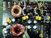
new version circuit:
now , the output square appear very clear and suddenly , but only one problem i just meet.
the square wave arrpear , that time , i saw the voltage of +/- side of square waveform more than +/-rail , and slowly change to normal +/- rail voltage.
so , i got the turn on tick sound , still .
can that solve by feedback circuit ??
new version circuit:
Attachments
Now , I have almost solved all problem.
1. The Delay turn on.
Use a 4093 to implement SD function.
2. The good 15v around -Vdd(-50v).
i use a another transformer output to make a AC20v around -Vdd.
So, when i turn off power , the ir2011's output will get down to --vdd.
early , i have turn off big tick sound that cause by i didn't let the ground of ir2011 connect to -vdd of main power.
when i turn off power , the ir2011's GND , ruse up to 0v , not -vdd. so , ir2011's lo-out rise to 0v and turn on low-side mosfet.
That why when i turn off power , the switching note rise to -vdd.
3. all of it were not using FEEDBACK circuit.
4. But now, turn on/off still get some tick sound , but very little.
I will connect the feedback circuit and test .
But i am not sure that does the resistor r27(47k) must use or not???
5. this is my new circuit
Attachments
Now , the circuit doesn't have feedback network is working very well.
I try to connect feedback circuit without R27(error amp feedback resistor).The C23 use 200p.
But when Ir2011 starting work after power on 5sec, the current sonsumption rise up to about 7A.
so , i try to reconnect R27 , but big current consumption still happened.
does anywhere in my circuit wrong ???
From the schematics, I guess your problem is that the way you have wired it, when you connect the feedback resistor, you will have POSITIVE feedback.
The way to know it is simple: swap the inputs to the IR2011. If that cures the problem, you had the polarities the wrong way.
33k fb resistor and 1k/200pF should work about right, but if you want some total gain you should reduce R28 to about 2.2k so total gain is 33K/2.2K=15 aprox.
And you can also increase R27 to, say, 150K to have more local feedback.
Best regards
OK , i will try it again .
And do you mean , the big current consumption was causing by the inputs of ir2011 connect wrong polarity from LT1016??
So , i just swap the output of nand gate to connect to ir2011.
It may solve the problem??
But i still have some question about some circuit.
1.what is the purpose of the RC low-pass filter on feedback network??
I test the wave on the point that after rc low-pass filter.
It still a +/-45v square wave , only it no ringing.
2. Why does the circuit is a POSITIVE feedback??
didn't i connect the feedback resistor to nagative input of error opamp??
I swap the inputs of IR2011 and connect the feedback circuit , the system can get starting success.
Now , I got only one problem is the turn on/off tick sound??
does it can be solved ??
Because i saw the volage of +/-rail not correct , when nand gate still shund down.
And when system work, the +/-rail get back to correct voltage.
I try to add a 3.9k/2w in +/-rail to get consumption to modify +/-rail voltage when the switching node have not had wave.
But it still didn't workly, still got "tick".
If i add subber between +rail to switching node and switching node to -rail , will it can help for tick ???
Althought the "tick sound" not very big , but it still get confuse with me.
so , i think if i can solve this problem , i will get a great experience.
First, let's concentrate in getting the basic operation of the circuit OK when it is estable, then we will worry about turn on / off.
Now it is clear that you had the PWM signals connected the wrong way and once you have inverted them you can connect feedback. Why? Because of the inverters chain (you take the feedback to the negative input of the error amp, but then you pass the error signal to the negative input of the comparator. Then you take the negative output to a level shifter that also inverts... etc, etc, so you end up with a increasing control signal when your output increases, so you had POSITIVE feedback.
You shouldn't get such a high square wave after R31/C28. Try increasing C28 to, say, 1.5 - 2nF. What is your sw. frequency now?
Have you measured the output waveform and listened to the background noise once feedback is connected? Did the DC offset disappear or at least become reduced? Is there less noise than before?
1. OK ,,, i understand why it is negative feedback.
2. so , what waveform and voltage should is after R31/C28 ??
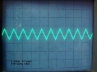
Now , my triangewave is 200KHz.The outpur square wave, of course, 200KHz too.
Why we have to use a RC low pass filter ??
I saw some circuit didn't have RC low pass fiter across the feedback network.
Only directly use a resistor connectg back to negative input of error opamp.
what's the purpose does the RC low-pass filter ???
3. Yes , after i connect the feedback , the output waveform's DC offsec have been to almost close to zero , under 50mV.
4. Yes, the background noise was disappear.It's very clear.
Only some current sound. But it is very small.
2. so , what waveform and voltage should is after R31/C28 ??
Now , my triangewave is 200KHz.The outpur square wave, of course, 200KHz too.
Why we have to use a RC low pass filter ??
I saw some circuit didn't have RC low pass fiter across the feedback network.
Only directly use a resistor connectg back to negative input of error opamp.
what's the purpose does the RC low-pass filter ???
3. Yes , after i connect the feedback , the output waveform's DC offsec have been to almost close to zero , under 50mV.
4. Yes, the background noise was disappear.It's very clear.
Only some current sound. But it is very small.
The RC filter is to attenuate a little bit the HF going into the error amplifier. It should have a cutoff frequency similar to the sw. frequency. 1K and 1nF give around 160KHz, perhaps slighty smaller C can do. (1k and 680nF).
Please try with several values until you get the best results.
To reduce noise, you can increase R27. What is the current value?
And C23 should be calculated such that the 1/(2*pi*C23*R27) = 30KHz aprox.
I recommend 150K and 33pF.
BTW: Please post a photo of your triangle waveform, I suspect it can't be very good with a TL084 and 200KHz freq.
1. you said "perhpas slighty smaller c can do(1k and 680nF).
do you write a wrong value ?? is 680pF ???
2. now the R27 is 180K. C23 is 200p. The Fc = 4KHz
Ok, i will try 150K and 33pF.
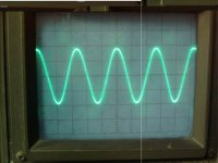
3. Now , i have used the LF347 to generate triangle wave.
but the triangle looks not like a linear triangle.
It looks like a sine wave , Like photo shown.
do you write a wrong value ?? is 680pF ???
2. now the R27 is 180K. C23 is 200p. The Fc = 4KHz
Ok, i will try 150K and 33pF.
3. Now , i have used the LF347 to generate triangle wave.
but the triangle looks not like a linear triangle.
It looks like a sine wave , Like photo shown.
Attachments
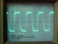
Yes, I made a mistake, I meant 680pF.
However, your 1k + 200pF waveform looks good, as long as the output of the error amplifier is not being saturated.
Your triangle is not linear at all. At that frequency, you need a faster opamp.
But... have you tried to inject signal and listen to the output? If so, what happens near clipping?
However, your 1k + 200pF waveform looks good, as long as the output of the error amplifier is not being saturated.
Your triangle is not linear at all. At that frequency, you need a faster opamp.
But... have you tried to inject signal and listen to the output? If so, what happens near clipping?
1. so , if output waveform voltage of the error opamp too high , should i have to lower the cutoff freq. ??
now is 180K/200p , Fc=4kHz
I found a question , if i didn't connect the LOAD.
When the ir2011 start working , the output of error opamp down to -5v , negative saturated.
But if i had LOAD , the whole system can work success.
so , did I have to change something or anything ??
Now , the output vlotage of error opamp almost +/-5v.
Looks almost saturated. Is that OK???
2. The LF347 still not fast enought ??
I used this prototype at http://www.play-hookey.com/analog/triangle_waveform_generator.html
He said the triangle's output is R1/R2 .
I use R1=10k and R2=100k , but my triangle voltage still not 15*1/10 = 1.5 , it become 20vpp triangle wave.
So , I always got confuse about it . did i connect wrong wire?
I have made sure for many times.
3. I inject the singal ever , when i didn't connect the feedback network. And It looks not BAD.
I only inject below 500Hz singal. if i don't forget , Its background seems clear for me.
I will try again in this circuit that connected the feedback network.
I do some summy for me.
1.the purpose of low pass filter of error opamp is to increase the stability , decrease noise.
The cutoff freq is equal to limit of input signal bandwidth.
2. The purpose of low pass filter in feedback network is to reduce HF noise , the cut off freq is equal to freq of triangle wave.
3. The total gain = feedback resistor form switching node / input resistor .
does it all right ??
I just see a LM4651's datasheet , there are some different explanin from above. But i don't really understand are they really different.
1. The low-pass filter in feedback network,the purpose is limiting the frequency of the input audio signal and feedback signal.
Maybe in datasheet's demo circuit was designed for subwoofer.
So , Its cutoff freq very low about 400Hz. (1M//470p)
2. The low-pass filter of error opamp , the purpose is remove the switching frequency and its harmonics.
But in the LM4651 , the low-pass cutoff freq set very low about 25KHz.
But its oscillation freq = 125KHz ~ 150KHz , why it set so low.??
And at its feedback network , It add a divider network first.
Let the feedback switching voltage divide 1/10 , then serial a low pass filter , and connect back to error opamp.
Why It divide the switching node voltage first ??
Does it help for anything ??
Don't worry too much about National stuff.
Your values are about right.
Yes, global gain is set by fb. resistor from sw. node / input resistor. That is true only when the inner gain is very high (gain of the error amplifier * gain of the output stage). If you use a high valued resistor such as 150K between -input and output of error opamp, as you are doing, you are ensuring this and the above is true.
The purpose of the "low pass filter" in the error opamp... well that's not a low pass filter exactly, it is an integrator with some DC gain provided by the 150K resistor. Its RC constant must be slightly higher than the audio band, but smaller than the sw. frequency. 50-60KHz is a good value.
The purpose of the lp filter in the feedback network is to reduce noise, that's true. It should be around the sw. frequency, although the best way to find its optimal values is simulation (or trial/error if you can't simulate). A good starting point is what you have.
How are you progressing with your amp?
- Status
- Not open for further replies.
- Home
- Amplifiers
- Class D
- hlpe ! Turn on get big current