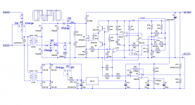
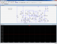
Here is a very unusual variable supply:
High voltage supplies can be a pain: they require special, high-voltage components, are dangerous to debug and to work with, and easily have reliability issues.This project is safe, tolerant, undemanding, and involves practically no high voltage business: everything is carried out on the safe side of a low voltage mains transformer, with the actual high voltage appearing practically only on the output node.
All the components are cheap and commonly available, and the supply can be dimensioned for practically any voltage or current output.
It is not quite a lab-grade supply: although the average output voltage is accurately regulated, it is only partially filtered, and there is no real current limitation: only the power is limited, and under 40V there is no limitation at all, and some other protection like a fuse has to be provided.
It is nevertheless a useful piece of workshop equipment for people working with tubes or SMPS's. It also has a few amazing tricks up his sleeve, more on that later.
The core of the circuit is basically a flyback converter, revisited by the lunatic asylum tech team.
Firstly, the step up function relies solely on the converter's boost ratio, and not on a transformer, and secondly, there is no explicit inductor, and the switching is performed directly on the AC raw from the ~30V transformer.
This looks like sheer madness: the switching is routed through a slow rectifier bridge, and uses the transformer's leakage inductance as a flyback inductor.
For those unfamiliar with magnetic technology, using a minor, parasitic parameter of a low frequency, iron transformer as a high frequency power inductor may look like a crazy idea.
In fact, this principle of "cryptoconverter"* is much sounder than it appears at first sight: the leakage inductance is practically independent from the core's nature, and the primary, shorted by a large capacitor, acts as a shield from the secondary for most of the iron.
The converter itself is of the current-mode variety, to cope with the straight AC, and is built around a LM339 quad comparator: this allows for a maximum of flexibility and avoids the use of a dedicated, harder to find specific IC.
The switch element is connected directly across the secondary via the rectifier bridge. It can be of a slow type, because it doesn't switch at a high frequency: it simply routes the switching signal.
This converter is controlled by an error amplifier consisting of half a LM358.
The control circuit has its own 12V supply, because it would be difficult to derive it efficiently from the main transformer.
Since the circuit relies on the transformer's leakage inductance, it has to be sufficient for proper operation. In practice, most types are suitable except toroidals.
EI types exist in two varieties: with the windings superposed or side-by-side.
Here, the side-by-side type is preferable, since it has a larger leakage inductance.
In the prototype, the transformer is not only of the side-by-side type, but in addition has a special form factor, which further increases the inductance.
This allows for a relatively low switching frequency (4KHz).
The output voltage ranges from 40V (converter becomes inactive) to more than 400V.
The output power is 80W, independent of the voltage setting. This is favorable compared to a classical supply, because the current mode converter acts partly as a PFC. It also reduces the ripple voltage compared to a plain rectifier+capacitor.
The iron becomes a little warmer on the secondary side, but nothing alarming.
One drawback of the direct boost topology is the demand on the switch element: it must be able to pass the full peak current of 6A, and to block the full output voltage, 400V here. This is not too much of a problem, as big switching FETs are available cheaply and easily.
*Because the main element remains hidden in another component
Attachments

You are right, it looks crazy. I tried googling for converter's boost ratio and cryptoconverter power supply, and came up blank. If you have any other search terms i can use to read about this type of design let me know.
That's a new concept, it is normal you don't find a lot on the subject: Une nouvelle classe de crypto-convertisseurs
The circuit shown is only a (working) example and can be altered, or serve as a base for a more complete supply: it would be possible to use it as a slave pre-regulator for a conventional linear supply, including a real current limitation.
Alternatively, it could be fitted with a simpler over-current trip circuit.
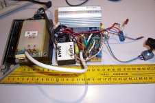
Here are some pics of my prototype: the transformer has an unusual form factor giving it a leakage inductance of ~4.5mH as seen from the secondary.
A more normal type is also usable, with a higher switching frequency.
For audio applications, it could be a bonus.
The applications of this topology are not limited to variable supplies: it could also be used in fixed-output circuits. I will give some ideas on this subject later.
The circuit shown is only a (working) example and can be altered, or serve as a base for a more complete supply: it would be possible to use it as a slave pre-regulator for a conventional linear supply, including a real current limitation.
Alternatively, it could be fitted with a simpler over-current trip circuit.
Here are some pics of my prototype: the transformer has an unusual form factor giving it a leakage inductance of ~4.5mH as seen from the secondary.
A more normal type is also usable, with a higher switching frequency.
For audio applications, it could be a bonus.
The applications of this topology are not limited to variable supplies: it could also be used in fixed-output circuits. I will give some ideas on this subject later.
Attachments


I am tempted to prototype one but with 3842 current mode chip or maybe even a 555 timer could be used ...
one question though: text book boost converters cannot remove 100Hz ripple, any ripple voltage present on the DC input voltage is also present on the output, because Vout = Vin + Vboost. Since you have no filter whatsoever on the input, doesn't that mean 100% ripple on the output ?
in case of 30V AC that would be some 40 volts.
If so, this could only be removed by post regulation. To produce clean 100v output, this converter would need to be set to 150v, and a subsequent linear regulator would have to burn 50v to get rid of the 100Hz ripple.
Or have I overlooked something ?
Strange it looked like a conventional flyback converter except there was no inductor, then the transformer leakage inductance came to mind.
@payloadde Flyback converters can remove ripple if the loop response is fast and the convertor has some headroom, the inductor is one pole of the filter, the filter capacitor is another, the PFC unit on modern SMPS's is an example of this. The ripple present on the output will depend on the size of the output filter capacitor and the regulator headroom at a given load.
@payloadde Flyback converters can remove ripple if the loop response is fast and the convertor has some headroom, the inductor is one pole of the filter, the filter capacitor is another, the PFC unit on modern SMPS's is an example of this. The ripple present on the output will depend on the size of the output filter capacitor and the regulator headroom at a given load.
That would be valid for a completely "dumb" converter, with no control or regulation.one question though: text book boost converters cannot remove 100Hz ripple, any ripple voltage present on the DC input voltage is also present on the output, because Vout = Vin + Vboost.
There is a filter: in this case, it is a post-filter, but the result is the same.Since you have no filter whatsoever on the input, doesn't that mean 100% ripple on the output ?
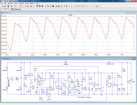
Suppose the supply is delivering 250V at its maximum power of 80W: that is 0.32A. With the 390µF filter cap, the ripple would be ~0.32*0.01/0.00039=8.2Vpp.
That is the absolute theoretical worst case, in reality the servo loop will improve on that, leaving less than 4Vpp ripple.
Note that the servo-loop is itself relatively "dumb" in its present state: it has a simple type II compensation (R21 C12 C9) having the optimum values for damping and settling time taking into account the tradeoffs necessary to operate with widely variable voltage and currents, but this optimum is neither necessary nor desirable:
Because the converter has to operate on a 100% modulated input @100Hz, the settling time is irrelevant, and the loop works in a suboptimal manner: it tries to follow the input signal, and this results in a ripple larger than is possible.
By manipulating the feedback signal, it possible to create a "smart" regulation: instead of trying to catch-up with the lack of output near the maximum of the waveform (like a peak rectifier does), it is possible to delay and to spread the energy transfer. This means that at the peak, there will still be a deficit compared to the reference, but this is made up later, and with some overshoot, to accumulate enough "reserve" to ride through the zero crossing. Using this strategy, it is possible to achieve a 1:10 reduction in ripple compared to the theoretical case, in this example it would leave less than 1Vpp ripple.
The problem is that the "strategy" has to be optimized for a limited range of current / voltage, and this is incompatible with a completely variable supply, which is why it isn't implemented here.
Yes, if you need a perfectly clean output, I mentionned the possibility of using the converter as a slave pre-regulator. You don't need a 50V margin: 5 to 10V would be sufficient, even less if you increase the 390µFTo produce clean 100v output, this converter would need to be set to 150v, and a subsequent linear regulator would have to burn 50v to get rid of the 100Hz ripple.
And now, let's go seriously bonkers...
After having read this topic, you might be thinking that things cannot go much crazier than that.
Think twice: you should never misunderestimate my abilities in that department...
This converter is completely "agnostic": it can feed happily on raw, unfiltered rectified AC, but it can as well use clean DC, from a battery for example.
All we have to do to convert this supply to a universal AC/DC version is add a function switch and a battery, or an external DC input.
The "choke" remains the same, the primary is just shorted to make sure the behavior is completely deterministic, and that's all.
You could for instance use this supply in a tube amplifier, making it as easily portable as any solid-state amplifier.
Attachments
A conventional SMPS with a PFC frontend also has this ability with no need for a switch, the bridge rectifier does it automatically. many other types of off line SMPS should also run from DC with no switching required.
If this circuit was modified to use a flyback transformer with the switching part run off line it could run AC/DC with no switch required.
Some portable televisions used a 12V supply which was supplied by a mains power transformer, there was a jack to power the television direct from 12V.
If this circuit was modified to use a flyback transformer with the switching part run off line it could run AC/DC with no switch required.
Some portable televisions used a 12V supply which was supplied by a mains power transformer, there was a jack to power the television direct from 12V.
Yes, in principle but as always the devil is in the details: details like the fact that a plain PFC will not be able to put out much less than ~350V.A conventional SMPS with a PFC frontend also has this ability with no need for a switch, the bridge rectifier does it automatically. many other types of off line SMPS should also run from DC with no switching required.
If this circuit was modified to use a flyback transformer with the switching part run off line it could run AC/DC with no switch required.
The output will also be non-isolated from the mains, and the control circuitry will also be mains-referenced.
And even the simplest of PFC's will already require one special inductor.
A solution is a full-blown isolated flyback converter, but this will require a specific transformer.
In addition, these solutions operate at voltages around 350V, and feeding these converters with a DC source of 1/10th this voltage will at least require a very substantial derating, if they accept to even start, which is not certain.
Everything being considered, these options are not very DIY-friendly.
The solution proposed here is simple, safe, flexible, and the main inductive component is a non-critical off-the-shelf 50 or 60Hz transformer, and will also work from 2 or 3 gel batteries (or even a single 24V one, with a reduced power).
Much more accessible to amateurs.
I just noticed that you have a separate transformer for the 12V winding. Does this winding have to be from a separate transformer.
Elvee this is one of the most interesting circuits I have seen in a long time that is possible to be built by poor amateurs like me. I still cut my "Electronic teeth" on vibrators and the OZ 4 rectifier tube . Seen them? I did the naughty thing during my final written exam using OC 26 transistors for a "Farm radio" in its power supply. I got my marks for "Originality" but I was told to use the old electromagnetic as that was what I was given. The question was to design a supply for 12 volt batteries I wonder what that old examiner would say looking at this in 1966?Yes, in principle but as always the devil is in the details: details like the fact that a plain PFC will not be able to put out much less than ~350V.
The output will also be non-isolated from the mains, and the control circuitry will also be mains-referenced.
And even the simplest of PFC's will already require one special inductor.
A solution is a full-blown isolated flyback converter, but this will require a specific transformer.
In addition, these solutions operate at voltages around 350V, and feeding these converters with a DC source of 1/10th this voltage will at least require a very substantial derating, if they accept to even start, which is not certain.
Everything being considered, these options are not very DIY-friendly.
The solution proposed here is simple, safe, flexible, and the main inductive component is a non-critical off-the-shelf 50 or 60Hz transformer, and will also work from 2 or 3 gel batteries (or even a single 24V one, with a reduced power).
Much more accessible to amateurs.

Last edited:
It isn't an absolute requirement, but it makes things easier: the voltages on auxiliary windings of the main transformer will be seriously perturbed, and unpredictably so: the ones close to the primary will be almost clean, but those coupled to the main secondary will have a severe switching contents.I just noticed that you have a separate transformer for the 12V winding. Does this winding have to be from a separate transformer.
All this is manageable, and most of my previous prototypes derived their power from the main winding, but here the peak voltage varies from 40V to more than 400V.
Since the control circuit needs less than 7mA, it would still be possible, but in some conditions, it would be necessary to dissipate 2.8W. It is doable, but a separate transformer is simpler.
Yeah, I played with them (and destroyed them out of abuse)Elvee this is one of the most interesting circuits I have seen in a long time that is possible to be built by poor amateurs like me. I still cut my "Electronic teeth" on vibrators and the OZ 4 rectifier tube . Seen them?
He would have dismissed the idea as insane and preposterous, even though the technology of the time would have already allowed it.I did the naughty thing during my final written exam using OC 26 transistors for a "Farm radio" in its power supply. I got my marks for "Originality" but I was told to use the old electromagnetic as that was what I was given. The question was to design a supply for 12 volt batteries I wonder what that old examiner would say looking at this in 1966?
I am going to illustrate the dimensioning using the values Rod has asked for:
Supposing it is the most common variety, EI with split primary and secondary windings, I can estimate the leakage inductance (seen from the secondary) to 1.28mH, using my statistical data (the best is of course to make an actual measurement).
Since the inductance is lower than in my example, and the voltage is higher, the frequency needs to be raised to keep the peak to average current ratio similar: a ~5x ratio will do.
C5 sets the frequency, it can be changed to 390pF, and the compensator cap C4 has to follow: it becomes 10nF.
The output filter cap has to be increased to accomodate for the 180W: it becomes 100µF.
The current sensing resistor has to be reduced too, to be able to deliver enough with 50V for 180W; it is lowered to 0.082Ω (the peak sense voltage across R2 reaches 1V).
The damper R1/C2 can be reduced to keep the dissipation reasonable.
The compensation network can be tweaked to take into account the various changes in parameters like the inductance, the frequency, the output cap, etc. It is not critical, with the original values the circuit would be overcompensated, but that is not a serious problem here.
The MOS must be able to pass in excess of 10A peak without too many losses, the original type would be suitable with a heatsink, a larger type could also be used.
In this case, it is a good idea to reinforce the gate driver by lowering R and using medium power transistors for Q1 and Q2.
The output diode should preferably be upgraded to a larger, ultrafast type.
That's about it: the other values can remain the same.
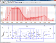
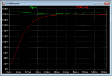
We can test the final result in sim: first the output voltage, with a ripple of ~2.5Vpp for 180W out, then the outlook of the current in the sense resistor for half a mains cycle, and finally the input voltage seen cycle by cycle: the frequency is ~21KHz.
And here is the sim file to play with:
First, we need to have an idea of the leakage inductance for the transformer in question.Excellent work!
It's always fun to use up some junk-box transformers.
How does it scale up? Can we use a 50V 250VA transformer and get 350V 180W?
Supposing it is the most common variety, EI with split primary and secondary windings, I can estimate the leakage inductance (seen from the secondary) to 1.28mH, using my statistical data (the best is of course to make an actual measurement).
Since the inductance is lower than in my example, and the voltage is higher, the frequency needs to be raised to keep the peak to average current ratio similar: a ~5x ratio will do.
C5 sets the frequency, it can be changed to 390pF, and the compensator cap C4 has to follow: it becomes 10nF.
The output filter cap has to be increased to accomodate for the 180W: it becomes 100µF.
The current sensing resistor has to be reduced too, to be able to deliver enough with 50V for 180W; it is lowered to 0.082Ω (the peak sense voltage across R2 reaches 1V).
The damper R1/C2 can be reduced to keep the dissipation reasonable.
The compensation network can be tweaked to take into account the various changes in parameters like the inductance, the frequency, the output cap, etc. It is not critical, with the original values the circuit would be overcompensated, but that is not a serious problem here.
The MOS must be able to pass in excess of 10A peak without too many losses, the original type would be suitable with a heatsink, a larger type could also be used.
In this case, it is a good idea to reinforce the gate driver by lowering R and using medium power transistors for Q1 and Q2.
The output diode should preferably be upgraded to a larger, ultrafast type.
That's about it: the other values can remain the same.
We can test the final result in sim: first the output voltage, with a ripple of ~2.5Vpp for 180W out, then the outlook of the current in the sense resistor for half a mains cycle, and finally the input voltage seen cycle by cycle: the frequency is ~21KHz.
And here is the sim file to play with:
Attachments

This circuit has great advantages for testing and lab work - really easy to re-adjust for different valves/tubes circuits, and all made out of cheap or junk-box parts.
Thank you very much for the worked example. This is the best of DIY audio - sharing some genuinely new and useful circuits. I'm sure I have a use for this - I had better measure some nice split-bobbin transformers I bought at a radio-rally (=hamfest). 24V 500VA for ~Euro 1.20 !
I assume that the LT1077 can be replaced by something cheaper -but would the LM358 suffice?
The basic concept can be improved/refined in many ways: one has already been mentionned, the manipulation of the FB signal to achieve lower ripple and/or or lower rms current for a given average current.
It is also possible to shield the main transformer from fast dV/dt's.
This has two advantages: it reduces the losses from eddy currents in the iron and in the copper, and it avoids the propagation of EMI/RFI associated with fast edges.
A way to implement this is to place an inductance of lower value than the leakage in series with the secondary. This is commpleted by a capacitor to form a second order filter.
Normally, such a configuration would require a substantial damping and the attendant dissipation to remove the ringing.
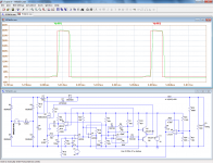
Here, the peculiar configuration of the switch allows for a lossless snubbering:
L2 is the additionnal inductor, having preferably good HF properties, C4 is the filter capacitor, and a recuperation diode D2 is added to clamp the overshoot/ringing to the output.
This provides the advantages of a heavy snubbering, without the severe losses it would normally cause.
The waveforms show the improvement: the red trace is the unfiltered waveform at the drain of the MOS, and the green one is taken behind the 150µH inductor.
It is also possible to shield the main transformer from fast dV/dt's.
This has two advantages: it reduces the losses from eddy currents in the iron and in the copper, and it avoids the propagation of EMI/RFI associated with fast edges.
A way to implement this is to place an inductance of lower value than the leakage in series with the secondary. This is commpleted by a capacitor to form a second order filter.
Normally, such a configuration would require a substantial damping and the attendant dissipation to remove the ringing.
Here, the peculiar configuration of the switch allows for a lossless snubbering:
L2 is the additionnal inductor, having preferably good HF properties, C4 is the filter capacitor, and a recuperation diode D2 is added to clamp the overshoot/ringing to the output.
This provides the advantages of a heavy snubbering, without the severe losses it would normally cause.
The waveforms show the improvement: the red trace is the unfiltered waveform at the drain of the MOS, and the green one is taken behind the 150µH inductor.
Attachments
Yes, in my prototype I have used a LM358. I used the LT1077 in the sim because it was directly available in LTspice's library, but it is non-critical: any general purpose op-amp having a common mode extending to 0V is suitable.I assume that the LT1077 can be replaced by something cheaper -but would the LM358 suffice?
I have also used a TLC272, it works transparently.
Use the simulated schematic only for change information relative to your case, there are some (unimportant) discrepancies with the actual physical circuit as shown in the first post.
Earlier, I hinted at the possibility to follow this circuit by a linear regulator.
Such an addition can provide a valuable enhancement in performance and usefulness. The two main benefits of such an upgrade are the elimination of the output ripple, and a deterministic current limitation.
Here is an example of such a suitable regulator: it is built around the half LM358 left free from the other circuit.
The circuit is somewhat unusual, because it is designed to integrate seamlessly with the preregulator: it is a negative regulator and it uses the same auxiliary 12V as the switching regulator.
The pass element is a cheap NMOS transistor.
The peculiar configuration requires the output voltage to be sensed in a bridge configuration. It is slightly inconvenient since it requires accurate matching of the two voltage dividers R2/R5 and R3/R4, but good matching is not difficult to achieve, and in view of the advantages this configuration affords, they can be tolerated.
The reference is upgraded from the initial 7812, it is now a TL431 having a 2.2K pot (R18/R19) to create the variable reference for the linear regulator.
A rudimentary current limiter is included: Q1 does the job, and in this example two ranges are provided, 100mA and 1A.
It also includes an indication of the current mode.
Since the opamp is too slow to reliably protect the MOS, a feedforward connection to the gate of the MOS via D1 is added (or from another point of view, D1 does the limiting and D2 prevents the saturation of the opamp: different description, same result).
To merge the two regulators, the inputs of the pre-regulator are reversed: it now senses the drop-out of the linear regulator on its (-) input, and regulates it against a 6V reference.
The simulation shows the operation of the tandem for a 200V output set by the main regulator. The LT1077 is used only for convergence reasons, in reality it can be a LM358 or 324, or TLC 272, etc
Note that this exact circuit has not been built, just simmed, but I have successfully used very similar variants.
Attachments
I have tested the linear post-regulator option:
After the inevitable material errors were corrected, the circuit worked immediately, but not perfectly: first, the switching regulation had become chaotic (literally, in the scientific sense): it had become a crude bang-bang regulator, functioning in an irregular manner.
This didn't prevent the correct operation of the circuit, since the linear regulator worked properly and eliminated the variations.
It was nevertheless intellectually disturbing, and probably not very healthy, so I decided to correct it.
That was not too difficult: the compensation of the switcher had not been modified, but with the new configuration, the loop gain had been multiplied by ~68x.
Curiously, it didn't show in the sim, but chaotic phenomenons are rather temperamental and difficult to catch.
Anyway, I simply had to correct the compensation network R25/C6 to 1µF and 10K. That completely solved the issue.
Next, I noticed that the output couldn't go below ~30V open circuit.
Some research showed that R21 was in parallel with the ballast and pulled the negative output.
Yet, I had been aware of this possibility: I had used large value resistors for the dividers, and had placed protection diodes on the input of U3, but this exact point somewhat escaped me.
It is true that the supply/ground configuration is rather unusual.
I corrected this problem with a diode in series and a bias resistor.
Then were the residues affecting the final output: both 100Hz and HF.
This was to be expected, as the layout/wiring was a complete non-sensical mess.
For the switcher, it didn't matter, but with the output cleaned by the linear reg, the residues had become unbearably visible.
I set out to correct the lay out. While working I had an unpleasant surprise: the main 390µF/450V filter cap had very unexpectedly remained charged, and I got a good bite.
The peculiar configuration switching + linear allowed the cap to remain charged, even with the load permanently connected to the final output: as soon as the mains disappears, the linear reg shuts down, and leaves the cap fully charged, waiting quietly for his victim, myself in this case.
I decided it was important to fit a discharge resistor to avoid further problems.
But I found it more convenient to make some more tests and make the clean-up in an orderly fashion, promising myself to be careful and do the mod ASAP. That was the lousiest idea I have had for a long time.
Well, you can guess what happened: as soon as I was busy with the clean-up, I completely forgot about the cap, that had been freshly reloaded to 400V.
I was reminded of its existence when I attempted to cut a ground wire (with uninsulated pliers) while firmly holding the MOS heatsink with my other hand: I got the jolt of the century (at least it felt like it).
It took me ten good minutes to recover.
I didn't postpone the discharge resistor anymore.....
I had quite a bit of work to do, to reroute the ground, use shielded cable for the MOS drain connection and the inputs of the linear regulator.
In the end, there were serious improvements: the 100Hz ripple was gone, and also most of the switching noise.
Some spikes of ~50mV remained, but that is inevitable with such a small board that had initially not been intended for this: the fast edges are still coupled inductively and capacitively, but now it is acceptable, and I will include a LC output filter when I build the thing into a case.
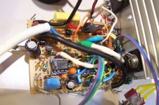
The result can be seen on the photo: it is impressively compact for a supply delivering more than 80W of useful DC power: 1.1A up to ~85V, decreasing linearly to 220mA at 405V.
The two level current limitation also works like a charm, and lights the LED when it needs to.
Quite satisfactory for a supply made of scrap material. The MOS I used in the linear section is an IRFP448 (not critical).
A word of caution to candidate-builders: do install the discharge resistor!!!
And be careful during the tests: with the special ground arrangements, it is easy to get messed up, and have the ground of a test instrument connected at a dangerous place. I can assure you that a 400V jolt is something to be remembered.
After the inevitable material errors were corrected, the circuit worked immediately, but not perfectly: first, the switching regulation had become chaotic (literally, in the scientific sense): it had become a crude bang-bang regulator, functioning in an irregular manner.
This didn't prevent the correct operation of the circuit, since the linear regulator worked properly and eliminated the variations.
It was nevertheless intellectually disturbing, and probably not very healthy, so I decided to correct it.
That was not too difficult: the compensation of the switcher had not been modified, but with the new configuration, the loop gain had been multiplied by ~68x.
Curiously, it didn't show in the sim, but chaotic phenomenons are rather temperamental and difficult to catch.
Anyway, I simply had to correct the compensation network R25/C6 to 1µF and 10K. That completely solved the issue.
Next, I noticed that the output couldn't go below ~30V open circuit.
Some research showed that R21 was in parallel with the ballast and pulled the negative output.
Yet, I had been aware of this possibility: I had used large value resistors for the dividers, and had placed protection diodes on the input of U3, but this exact point somewhat escaped me.
It is true that the supply/ground configuration is rather unusual.
I corrected this problem with a diode in series and a bias resistor.
Then were the residues affecting the final output: both 100Hz and HF.
This was to be expected, as the layout/wiring was a complete non-sensical mess.
For the switcher, it didn't matter, but with the output cleaned by the linear reg, the residues had become unbearably visible.
I set out to correct the lay out. While working I had an unpleasant surprise: the main 390µF/450V filter cap had very unexpectedly remained charged, and I got a good bite.
The peculiar configuration switching + linear allowed the cap to remain charged, even with the load permanently connected to the final output: as soon as the mains disappears, the linear reg shuts down, and leaves the cap fully charged, waiting quietly for his victim, myself in this case.
I decided it was important to fit a discharge resistor to avoid further problems.
But I found it more convenient to make some more tests and make the clean-up in an orderly fashion, promising myself to be careful and do the mod ASAP. That was the lousiest idea I have had for a long time.
Well, you can guess what happened: as soon as I was busy with the clean-up, I completely forgot about the cap, that had been freshly reloaded to 400V.
I was reminded of its existence when I attempted to cut a ground wire (with uninsulated pliers) while firmly holding the MOS heatsink with my other hand: I got the jolt of the century (at least it felt like it).
It took me ten good minutes to recover.
I didn't postpone the discharge resistor anymore.....
I had quite a bit of work to do, to reroute the ground, use shielded cable for the MOS drain connection and the inputs of the linear regulator.
In the end, there were serious improvements: the 100Hz ripple was gone, and also most of the switching noise.
Some spikes of ~50mV remained, but that is inevitable with such a small board that had initially not been intended for this: the fast edges are still coupled inductively and capacitively, but now it is acceptable, and I will include a LC output filter when I build the thing into a case.
The result can be seen on the photo: it is impressively compact for a supply delivering more than 80W of useful DC power: 1.1A up to ~85V, decreasing linearly to 220mA at 405V.
The two level current limitation also works like a charm, and lights the LED when it needs to.
Quite satisfactory for a supply made of scrap material. The MOS I used in the linear section is an IRFP448 (not critical).
A word of caution to candidate-builders: do install the discharge resistor!!!
And be careful during the tests: with the special ground arrangements, it is easy to get messed up, and have the ground of a test instrument connected at a dangerous place. I can assure you that a 400V jolt is something to be remembered.
Attachments
Last edited:
How are you going to get 1.28 mH of leakage inductance on the secondary side of the transformer? Also on the post that showed this inductor, the secondary voltage was shown as 75 volts peak, not 42.4 as would be the case for 30 Vrms that you showed earlier.
You have probably mixed up the two design examples I have provided (not your fault, I wasn't very clear in which was which).How are you going to get 1.28 mH of leakage inductance on the secondary side of the transformer?
All of the actual data, pertaining to my physical example are based on a 30V transformer. That one has been measured (4.5mH leakage) and simulated in the posts relative to my own prototype, the one shown in the pics.
I have also dimensioned another example for Rod Coleman, based on the data he provided: a 50V transformer. There, I have used generic data, based on the most common type of EI transformer he is susceptible to use (1.28mH leakage).
The difference may look abnormal: the lower voltage transformer (mine) has a higher leakage than his.
There are two reasons: his has a higher power, but more importantly, mine has an unusual form factor, as you can see from the pics. This, combined with the split bobbins creates a much higher leakage than usual.
See above.Also on the post that showed this inductor, the secondary voltage was shown as 75 volts peak, not 42.4 as would be the case for 30 Vrms that you showed earlier.
Note that everything regarding the 50V transformer (~75V peak) is an estimation, has not been tested and needs to be validated physically.
Last edited:
- Status
- Not open for further replies.
- Home
- Amplifiers
- Power Supplies
- High Voltage Variable Supply on a Shoestring