Instead of using back-to-back transformers, would it be possible to drive the step up transformer from a switching DC supply like this?:

Or maybe best to connect the center tap to VCC and use P chans.
I have a page here: https://www.diyaudio.com/community/threads/12v-pure-sine-wave-inverter-using-op-amps.417438
Or maybe best to connect the center tap to VCC and use P chans.
I have a page here: https://www.diyaudio.com/community/threads/12v-pure-sine-wave-inverter-using-op-amps.417438
👍 I call them Stabilizers too.IMO its a stabilizer, not a regulator.
This is perfectly appropriate for the Valve/Tube world - historically, the use of voltage stabilisers (based on gas tube reference voltage) and current stabilisers (Barretters) were perfectly normal. These were often designed wthout any separate closed loop, just like the Power-MOS follower based example shown in this thread.
But I (personally) only use the word regulator to describe a supply with a closed loop.
A Voltage-reference + Power Follower can make an excellent power supply for Anode or G2 supplies. My versions are plenty stable enough: less than ±1% is achievable with design effort. Compare this to the ±10% power utilities are allowed here (UK).
Also, low output impedance is easily realised: with a 100mA load and a good FET, small-signal Z is ca. 1Ω.
IOW, this is a huge improvement in performance compared to passive supplies, and also means that expensive parts like valve-rectifiers, startup delay timers, boutique capacitors and (worst of all) large iron chokes are made irrelevant - no longer required.
With Class-A SE anode supplies (where the whole of the signal-current swing is carried by the series elements of the anode supply), the FET Stabiliser is much prefereable to a closed-loop regulator. In this position, closed loop regulators take over the sound of a fine SE amplifier - sucking the life out of it. I found this 25 years ago with my 300B-SE, and subsequently found other constructors had the same reaction. No such problem with the FET stabiliser though...

After discussion mainly about the name,
is there anyone who has built this circuit?
I think my idea is not too bad.
Escpecially for the Tube-people 🙂
I have been using something similar for years. I use an IXYS 10M45S in place of the CCS, or just a resistor and capacitor in non critical applications. As wg_ski pointed out the usual place to use these is for a screen grid power source where absolute regulation is not needed.Zener diode based “regulators” are still “regulated” compared to just an RCRC filter off the raw supply. Good enough for screen voltages or preamp stages. And the SS version is good enough to power op amps. Neither usually needs .1% or less line/load regulation.
I still call it a regulator. It walks like a duck, quacks and likes water.
The mosfet used for the follower must be capable of steady state DC power dissipation, and many of the new HV parts designed for SMPS will fail to a short if subjected to long term DC dissipation. TV sweep tubes can draw huge current pulses on their screen grids when driven into clipping where the plate voltage may momentarily drop below the screen voltage. Many current mosfets (especially those from ON Semi) will fail to a short from this transient even though they remain well within their published ratings. This puts full B+ on the screen grid making for a short unhappy life for the tube. A large resistor in series with the drain of the follower can help, as it drops the drain voltage during overload.
Secondary breakdown effects DO exist in mosfets, though the mechanism is somewhat different from those seen in BJT's. Beware of parts that do not put SOA curves in the data sheet, or where the DC curves are equal to the max power dissipation spec. I use IXYS D2 depletion mode mosfets or better still (but pricey) their Linear L2 parts with Extended FBSOA.
For absolute tube purists who still believe that all silicon is evil, this circuit can be built with vacuum tubes. Some high Gm pentodes can make a reasonable CCS and VR tubes like the 0A2 can sub for the zeners.
Yes, Legacy Fairchild and IRF types fare much better than newer ON or Infineon types for linear operation. There is a reason people are still using IRF240/9240 for class AB amps. They work. They don’t go bang. They still do have second breakdown, but like MJ15024 it doesn’t kick in till 80 volts or so. Unfortunately, won’t work to drop 500V down to 200 (Only 200V rated Vds).
IXYS makes some really good IGBTs I’ve been meaning to try out.
IXYS makes some really good IGBTs I’ve been meaning to try out.
It's unlikely to be an obstacle, if the FET is selected for generous DC SOA.The output impedance is limited by Rds(on) of Q1
Other than the piece-cost, there is no disadvantage to choosing a large-capacity, wide-SOA device. The increased capacitances that come with a husky big FET don't matter for this application, unlike with switching, or even linear voltage-signal applications.
Signs of a suitable SOA diagram: A line for DC should be present (indicates linear operation capability); and the Right-hand of the SOA plot should not have a sharper gradient at higher voltages (this indicates the FET-analogue of the BJT 2nd Breakdown parameter). Select a FET that can manage a DC stress of the chosen O/P voltage AND more than the load current, simultaneously. It should not normally face such a stress, but might do under fault conditions.
Last edited:
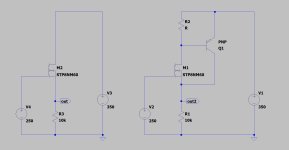
Agree. Nobody's home to watch the output voltage and do something about it.@lineup, with all due respect, I am not sure why you call this a regulator. Nothing is regulated, it's a source follower (sometimes fancy-named capacitor multiplier).
There is no mechanism to regulate; to correct the gate voltage for output voltage drop.
Jan
The problem with FETs and SOA is that they are NOT always as advertised. The data sheet may show fantastic SOA but they may be lying, or at least, mistaken. Switching devices often show purely thermally limited SOA which is more often than not, untrue. When they do show actual curves, a 600W FET might be good for 30W (not 30A) at VDS=20.It's unlikely to be an obstacle, if the FET is selected for generous DC SOA.
Other than the piece-cost, there is no disadvantage to choosing a large-capacity, wide-SOA device. The increased capacitances that come with a husky big FET don't matter for this application, unlike with switching, or even linear voltage-signal applications.
Signs of a suitable SOA diagram: A line for DC should be present (indicates linear operation capability); and the Right-hand of the SOA plot should not have a sharper gradient at higher voltages (this indicates the FET-analogue of the BJT 2nd Breakdown parameter). Select a FET that can manage a DC stress of the chosen O/P voltage AND more than the load current, simultaneously. It should not normally face such a stress, but might do under fault conditions.
I disagree, a source follower have an internal feedback mechanism, if the output voltage drops the mosfet will conduct more current , of course the feedback it’s low , a bjt would be better.Agree. Nobody's home to watch the output voltage and do something about it.
The choice of a Power FET for this application requires Linear operation as an intended capability - indicated by a DC plot of SOA, and no sign of the pseudo "2nd breakdown" at higher voltages. So pure-play switching devices - which do not plot a DC SOA - are not advisable here at all. This is an effective exclusion of whole ranges of devices, or even the entire repertory of some manufacturers.The problem with FETs and SOA is that they are NOT always as advertised. The data sheet may show fantastic SOA but they may be lying, or at least, mistaken. Switching devices often show purely thermally limited SOA which is more often than not, untrue. When they do show actual curves, a 600W FET might be good for 30W (not 30A) at VDS=20.
It remains up to the circuit designer to test their work, including under reasonably foreseeable fault condtions. These tests may well apply stresses deep into the DC or transient SOA regions. Use dummy loads, and understand what SOA points the power device can repeatedly withstand, before installing the stabiliser into its intended position. It's not a trivial task; but that's OK if one is a pro.
That's like saying that a resistor has feedback, you increase the voltage across a resistor and the current increases.I disagree, a source follower have an internal feedback mechanism, if the output voltage drops the mosfet will conduct more current , of course the feedback it’s low , a bjt would be better.
But it's stricktly a linear process, just as pulling more current out of a FET source increases the Vgs.
With all due respect, but your post seems to show an incomplete understanding of what feedback is.
Jan
But the problem is they often show a perfect DC SOA and it’s not true. I’d rather use a device whose data sheet does show the voltage effects, because they are at least admitting the issue and measured it. There are varying degrees of it, and the bottom line is you end up looking for parts that show a relatively high Qg for a given die area, and relatively high Rds on - rather than the best switch on the market. I’ve resorted to FET/bipolar darlingtons, because MJL4281 can beat most high voltage FETs. TIP50 is pretty good for the money/size, too. Keeping VDS/Vce down is the best solution, but not always possible.
I might expect that of recently designed switching FETs, but not from large-area FETs, rated for linear operation.But the problem is they often show a perfect DC SOA and it’s not true.
If your experience is different, tell us some examples of the part numbers, and how you measured where you were on the SOA surface when the sample failed.
We're not looking for the best switch. It's wide-SOA linear operation we need:you end up looking for parts that show a relatively high Qg for a given die area, and relatively high Rds on - rather than the best switch on the market.
Qg = don't care. Large Die Area, Large capacitances = No problem.
Perhaps you are losing sight of the application here.
the source of the Mosfet in this circuit is the output but it´s also the (inverted) input, as the output current is dependent of the voltage between the gate and the source (Vgs) , it´s a current fedback amplifier with a gain of 1 ( well it would be 1 if the MOSFET transconductance was infinite ) ,I'm sure if you think about it you'll see it too.That's like saying that a resistor has feedback, you increase the voltage across a resistor and the current increases.
But it's stricktly a linear process, just as pulling more current out of a FET source increases the Vgs.
With all due respect, but your post seems to show an incomplete understanding of what feedback is.
Jan
No I’m not losing sight of the application. Try finding a 500 V FET these days that’s suitable for linear operation. Slim pickings. I get better power handling out of a 36W, 5A unit with 1.3 ohms rds than a 20 amper that’s supposedly good for 300 watts. And they change which part numbers are even offered as often as we change underwear. So what you can get today may go away tomorrow.
Even the IRFP240 is only good for full power up to about 70 volts or so, and after that it falls off. Data sheets never showed that. And those are GOOD for linear operation. They just go downhill from there. Best “modern” variety I’ve seen is the IRF4227 family. Full power to 55V, actually reflected in the data sheet too. But only 200V class, so possibly no dice as a screen regulator.
Even the IRFP240 is only good for full power up to about 70 volts or so, and after that it falls off. Data sheets never showed that. And those are GOOD for linear operation. They just go downhill from there. Best “modern” variety I’ve seen is the IRF4227 family. Full power to 55V, actually reflected in the data sheet too. But only 200V class, so possibly no dice as a screen regulator.
No I don't see that and I see no explanation how this would work either.the source of the Mosfet in this circuit is the output but it´s also the (inverted) input, as the output current is dependent of the voltage between the gate and the source (Vgs) , it´s a current fedback amplifier with a gain of 1 ( well it would be 1 if the MOSFET transconductance was infinite ) ,I'm sure if you think about it you'll see it too.
If you drive the gate with a signal, increasing the gate voltage increases the source current, which will increase the source voltage, which counteracts the rise in Vg and is a case of (local) feedback.
In the case of a capacitor multiplier, where Vg is (ideally) constant, pulling more load current out of the source increases Vgs but there is nothing that provides counteraction.
It is strictly linear and there is no feedback mechanism that somehow 'compensates' or counteracts the drop in output voltage.
Another way to look at it is to realize that (negative) feedback always decreases the forward gain. There is nothing in the capacitance multiplier that has that effect, the forward gain is already below 1.
Jan
You can increase the open loop gain just by adding a resistor and a BJT (or MOSFET), in that case you would have less output impedance, the negative feedback mechanism is exactly the same.True, but the effect is minuscule.
Attachments
better stock up on the ones you like (just as we do with the Valves themselves). They don't go stale.Try finding a 500 V FET
Infineon IRFP240 does not even offer a DC SOA, so you can't complain if it fails in linear operation.Even the IRFP240 is only good for full power up to about 70 volts or so
Just like in the days of valves, component internals can be changed - IF it still conforms to the data sheet. You have no comeback if you rely on performance that was not guaranteed.
As I have already said, it's up to the designer to verify that their work is reliable with the parts specified. Nobody else is to blame.
And, If you have a company making some product with scarce parts, you better buy all the known-good types you can and put them in the company safe.
I don't see any evidence of manufacturer's deception over SOAs in data sheets.
The 240 is good as a linear amplifier - as a class AB running on +/-70V, which is pretty much what fet-o-Philes do with them. Their voltage limitations were just never reached in traditional applications. The second-breakdown-like phenomena weren’t immediately apparent even to manufacturers until modern HV types (and even the 50 to 75 volt super high current ones) were tried in linear apps - with spectacular failures. Some data sheets were updated. Others were not.
Regardless, I’ve simply given up on trying to find FETs that can handle more than a handful of watts at 200+ volts. If that’s needed I use a bipolar. My tube applications get load tested into a resistor first. I normally don’t go running low(er) voltage screens off the main winding. A lower voltage tap is the right place to run it but you have to be willing to wind transformers, or stack multiple off the shelf units. Preamps drawing 10 milliamps in class A, not the 200 mA screen peaks, can effectively be run off a FET regulator that drops 300V.
Regardless, I’ve simply given up on trying to find FETs that can handle more than a handful of watts at 200+ volts. If that’s needed I use a bipolar. My tube applications get load tested into a resistor first. I normally don’t go running low(er) voltage screens off the main winding. A lower voltage tap is the right place to run it but you have to be willing to wind transformers, or stack multiple off the shelf units. Preamps drawing 10 milliamps in class A, not the 200 mA screen peaks, can effectively be run off a FET regulator that drops 300V.
- Home
- Amplifiers
- Power Supplies
- High Voltage power supply, source follower and ripple eater for TUBES