Any questions you /we may have about the commercial example of an audio power amplifier in this thread should be put directly to the Cambridge Audio engineers, this print can be found in the azur 550, 650, 651 A models.
Dear Azubinski,
Assuming that you, as a consulting company (hypothetical), were commissioned to re-dimension this 25W amplifier, but to maintain its topology, what would be your suggestion?
kind regards,
HBt.
Assuming that you, as a consulting company (hypothetical), were commissioned to re-dimension this 25W amplifier, but to maintain its topology, what would be your suggestion?
kind regards,
HBt.
C9 and C10 need to be more than 16V. The voltage amplifier is very sensitive to the difference between the supply rails. I would not build this amplifier.
Ed
Ed
Your statement is very interesting Ed, because of the why! Why would you not implement this design proposal as it was published?
It must be easy for us (today) to eliminate the obvious and apparent flaws of the circuit - as a result we would have a small, simple, well thought-out 25 watt hi-fi amplifier with current components and devices of our choice.
The template leaves enough room for our own interpretations, or rather explanations - modifications.
C9 and C10 will burn out due to overvoltage. The authors may have used a regulated supply and did not notice the ripple sensitivity. They were lucky that the amplifier worked.
The measured distortion is entirely consistent with the amount of negative feedback used.
Ed
The measured distortion is entirely consistent with the amount of negative feedback used.
Ed
BC548/549 in the IPS are 20V VCE and BC327/337 are 45V while the voltage swing can be close to 48V, that s hasardous
choice of devices, also they use a resistance rather than a CCS for the differential, wich make the THD figures dubbious,
with a resistance you ll hardly get H2 lower than -80dB.
Also the offset correction voltage is not filtered so they inject the supply noise at a rate of -40dB in the non inverting input,
there should be a capacitor in parralel with R12.

This amp is stabilised by the 15pF lead lag cap, if it s removed it oscillate, and even with the cap there s still
a pole that display a peak at 1.5MHz in the frequency response, THD is quite low actually but at the expense
of inconditional stability.
Idle power of the thing is about 16W since the class A driver is implemented at the final output transistors level,
an intermediary driver stage would have been necessary for class A drive at a lower standing current.
Then now is the time to breathe the breath of this decade into this little amplifier. Let's bring it to life, with components and values that make it play reliably.
🙂
The criticism voiced in the forum is obvious and justified at first glance - but not a criterion for rejection.
🙂
The criticism voiced in the forum is obvious and justified at first glance - but not a criterion for rejection.
Would you like to post your simulation here and share it with us?This amp is stabilised by the 15pF lead lag cap, if it s removed it oscillate, and even with the cap there s still
a pole that display a peak at 1.5MHz in the frequency response, THD is quite low actually but at the expense
of inconditional stability.
kindly,
HBt.
If we want to continue knitting the thread and there is (minimal) interest in a real implementation, I suggest that we use this nomenclature


in mutual exchange for the time being.
We can also immediately see here what measures have been taken to ensure that a VCE_max of less than 48Vdc is not a real problem. The question naturally arises as to why the author of the article did not use more voltage-resistant BJTs and the tiny BDs in the output stage.
C2 and C3 do not go up in smoke because an MKT or MKP type is used, known to have voltage strengths of 63Vdc in the worst case.
The time constant of approximately R24*C5=22msec is also not necessarily a relevant point of criticism, but leaves enough room to live out the play instinct. Two additional voltage dividers are connected upstream, VR2 -> R25&R26 ---> R24( & re_Q4 & XC5).
R3,8,14,15 do the rest.
The circuit will work, but we can drill it out. Let's just do it together 😉.
You re welcome, here a few graphs that i will shortly comment.Would you like to post your simulation here and share it with us?
kindly,
HBt.
Given that this design date from 1980 i strongly suspect that the designers where influenced by Matti Otala,
who was famed at this time, because he once stated that an amp OLG BW should be 20kHz, wich is the case here
with a 77dB OLG that extend to this frequency, but so far i dont remember that he advised for LG (loop gain)
as high as 50dB at this frequency, wich is the case in this amplifier and is too much for inconditional stability.
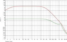
In the first graph you have the OLG and CLG with the pole displaced at 1.5MHz by the lead lag cap.
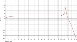
On the second is the CLG without lead cap with pole at 550kHz.
Third is the output signal at 20V pk and 10V pk without lead lag cap and showing the oscillation.
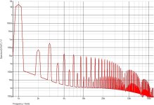
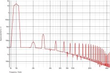
Fourth and fifth are the THD at 1kHz and at 10KHz in normal condition, that is with the lead cap and excess LG.
Hope this help your improvement of this design.
Attachments

Thank you very much wahab,Given that this design date from 1980 i strongly suspect that the designers where influenced by Matti Otala,
who was famed at this time, because he once stated that an amp OLG BW should be 20kHz, wich is the case here
with a 77dB OLG that extend to this frequency, but so far i dont remember that he advised for LG (loop gain)
as high as 50dB at this frequency, wich is the case in this amplifier and is too much for inconditional stability.
(...)
yes - the spirit of the times and the doctrines are clearly recognizable. The TIM, TID vs. THD ... debate and the SR number.
In a quiet hour I will also feed the simulator - and probably end up with the well-known Blameless architecture in the optimization process - but that's exactly what I don't want.
I would simply like to experience listening and thus also trace back the color of the /that time. Somehow I am also concerned with the relevance of our data, simply the economy - kiss principle.
About simplicity.
I don't know what the big deal is about this abstract?Mr. Joseph M. Diamond and published in 1969, it is commonly called the [D|d]iamond buffer:
https://ieeexplore.ieee.org/abstract/document/1162052
And since very few people now know about Mr. Diamond, it can be assumed that the name is so old that its origin has been lost.
The bubble has burst.
Dear @cumbb,The advantage of the circuit in #1 is that both half-waves see the same two complementary transistors, so their audible different characters can be heard in both half-waves: The half-waves sound audibly less different.
Q5 and Q6 are not "identical". The largest audible difference between the half-waves is created here.
You are so entertaining that I have decided to take you off my ignore list again. Your comments are sometimes a bit annoying but also totally funny.
Now please give yourself a jolt and help me solve the shortcoming you pointed out of Q5 & Q6 only occurring once each.
Incidentally, we are correctly talking about "oscillations /Schwingungen" and not "waves /Wellen".
HBt.
And I always thought it was called a diamond buffer because it was arranged in a diamond (in the schematic, of course). But some around here probably think a diamond buffer is someone who polishes stones. And if one didn’t have it drilled into their head about who invented the telephone, one would think Bell Telephone had something to do with the signal that a call was coming in.
Hey, we could add a current mirror to Q5 and Q6, get the transistor count accurate again, and help with the poor PSRR at the same time, at least in theory…. When one goes to build a “high performance” amplifier and you go do a different topology for the sake of being different, there is always something that you miss and it doesn’t work out as planned. 99.99% of the time. “Different never works.” That residual .01% is where innovations come from, and those are as rare as diamonds. Take them when you find them, and throw the rest back.
Hey, we could add a current mirror to Q5 and Q6, get the transistor count accurate again, and help with the poor PSRR at the same time, at least in theory…. When one goes to build a “high performance” amplifier and you go do a different topology for the sake of being different, there is always something that you miss and it doesn’t work out as planned. 99.99% of the time. “Different never works.” That residual .01% is where innovations come from, and those are as rare as diamonds. Take them when you find them, and throw the rest back.
The PSRR problem comes from the signal being referenced to both rails simultaneously even at low frequencies (C2 and C3 in post #30). This design cannot tolerate ripple.
Ed
Ed
Before this thread becomes a comedy, I'll give the project a name. I decide: “little amplifier, you shall be called Tim from today”!
But Ed, this little problem can be solved immediately. We divide R10 and R30, insert a Zener diode ... we simply ensure a clean supply voltage to the base of Q5 & Q7.The PSRR problem comes from the signal being referenced to both rails simultaneously even at low frequencies (C2 and C3 in post #30). This design cannot tolerate ripple.
Ed
- Home
- Amplifiers
- Solid State
- high performance 25W PowerAmp