Hello
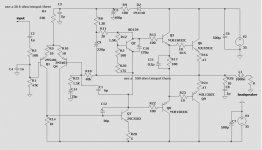
Here's a simple but very good sounding 50 watts amp.
To keep it simple, there is no CCS and current mirror.
One of the most important section of any amplifier are the VAS (voltage amplification section), that section need to be fast with a low capacitor value. A slow VAS will reduce the slew rate of the amp, meaning reducing the speed of the amp.
The VAS need a fast transistor (the ft), and with a low output capacitance (the cob).
Here's the recommended NPN VAS transistors:
2SC3423 TO-220 ecb, cob: 1.8 pf, ft: 200 mhz
2SC3600 TO-126 ecb, cob: 1.4 pf, ft: 400 mhz
2SC3955 TO-126ML ecb, cob: 1.9 pf, ft: 300 mhz
KSC3503 TO-126 ecb, cob: 2.6 pf, ft: 150 mhz
2SC2911 TO-126 bce, cob: 3 pf, ft: 150 mhz
2SC2911 TO-126 bce, cob: 3 pf, ft: 150 mhz
BD139 are not very good for VAS Transistors, I don't recommend it.
VAS lag comp capacitor for this amp are C12 and the value is 30 pf, too high value will slower the amp.
There is C1, a phase lead capacitor, this capacitor help the amplifier to be more able to drive difficult load loudspeakers, and the value is 6pF.
C11 are the suck-up capacitor between the two drivers, and with R17, it's removes the HF artefacts of the output stage.
R4 are the output offset adjustment, use a 50 k ohm trimpot there, and adjust it for the lower dc voltage at the amp output.
R20 are the bias adjustment, use a 500 ohm trimpot there, and adjust it for a bias of 60 ma for low crossover distortions, R2 are there in case the trimpot become defect.
D2 help to keep the input and vas stage relatively independent from voltage variations from the output stage current demand.
The distortion of that amp are arround .008 %
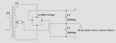
For best result, all ground should be connect between the two big capacitor of the power supply, look at the image.
I have a limited times to use my low speed internet, so it coud take times for me toreply to any questions.
Bye
Gaetan
Here's a simple but very good sounding 50 watts amp.
To keep it simple, there is no CCS and current mirror.
One of the most important section of any amplifier are the VAS (voltage amplification section), that section need to be fast with a low capacitor value. A slow VAS will reduce the slew rate of the amp, meaning reducing the speed of the amp.
The VAS need a fast transistor (the ft), and with a low output capacitance (the cob).
Here's the recommended NPN VAS transistors:
2SC3423 TO-220 ecb, cob: 1.8 pf, ft: 200 mhz
2SC3600 TO-126 ecb, cob: 1.4 pf, ft: 400 mhz
2SC3955 TO-126ML ecb, cob: 1.9 pf, ft: 300 mhz
KSC3503 TO-126 ecb, cob: 2.6 pf, ft: 150 mhz
2SC2911 TO-126 bce, cob: 3 pf, ft: 150 mhz
2SC2911 TO-126 bce, cob: 3 pf, ft: 150 mhz
BD139 are not very good for VAS Transistors, I don't recommend it.
VAS lag comp capacitor for this amp are C12 and the value is 30 pf, too high value will slower the amp.
There is C1, a phase lead capacitor, this capacitor help the amplifier to be more able to drive difficult load loudspeakers, and the value is 6pF.
C11 are the suck-up capacitor between the two drivers, and with R17, it's removes the HF artefacts of the output stage.
R4 are the output offset adjustment, use a 50 k ohm trimpot there, and adjust it for the lower dc voltage at the amp output.
R20 are the bias adjustment, use a 500 ohm trimpot there, and adjust it for a bias of 60 ma for low crossover distortions, R2 are there in case the trimpot become defect.
D2 help to keep the input and vas stage relatively independent from voltage variations from the output stage current demand.
The distortion of that amp are arround .008 %
For best result, all ground should be connect between the two big capacitor of the power supply, look at the image.
I have a limited times to use my low speed internet, so it coud take times for me toreply to any questions.
Bye
Gaetan
Attachments
Last edited:
The distortion of that amp are arround .008 %
At what condition (the measurement)?
It might be difficult to implement the always mandatory current protection and current/voltage (SOAR) protection
At what condition (the measurement)?
Hello
With a LTspice simulation, knowing that's a theorical number, but most of the time the simulation thd was very close to the thd of the constructed amplifiers.
Bye
Gaetan
Attachments
Member
Joined 2009
Paid Member
These are very nice amplifiers, this topology was the first kind I ever built in this hobby and is still going.
Hello
With a LTspice simulation, knowing that's a theorical number, but most of the time the simulation thd was very close to the thd of the constructed amplifiers.
Usually the real one is worse because simulators assume perfect PCB.
In simulator the THD is at 1kHz, may be with 1V input that correlates with 3W or something. Real commercial amplifiers specify THD as the maximum THD at rated power from 20Hz to 20kHz. I think the high standard is around 0.07% at 100W. With such Lin topology, 0.08% at 50W is very good. I think top Sony receiver (ES) has it around 0.08% at 80W or something (JFET current source).
Usually the real one is worse because simulators assume perfect PCB.
The simulation models also neglect a lot of second and third order effects in the various devices. The models may fit well with actual device behaviour in most operating regions, but not so well in others. That's not an indication that modelling is bad, just that it's a huge challenge to write models that are accurate under all operating conditions and will allow the simulator to converge as well.
That said, one can usually find a correlation factor between simulation and reality. One thing is certain: If the simulator predicts horrible THD, the circuit will likely show poor performance as well.
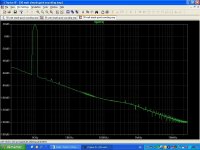
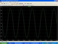
In the posted FFT, the harmonics are barely above the noise floor of the analysis. I suggest increasing the FFT length and matching the step size of the simulation to the FFT bin size. This will likely allow you to resolve the harmonics a bit better.
Tom
That said, one can usually find a correlation factor between simulation and reality.
Yes, but such single THD specification is IMHO useless, especially if it is used to represent the amplifier's quality.
This amp is using bootstrap, so THD comparison is valid only with similar topology, which is not widely used by expensive amplifiers. Replacing with CCS will improve measured performance but subjectively many prefers the bootstrap (and resistor biasing) even if the distortion is higher. (This makes comparison even more difficult)
Not correct, I have found on real amps that replacing with CCS increases odd harmonics although the overall thd is sometimes lower. of course every non-linear active device must increase odd harmonics.Yes, but such single THD specification is IMHO useless, especially if it is used to represent the amplifier's quality.
This amp is using bootstrap, so THD comparison is valid only with similar topology, which is not widely used by expensive amplifiers. Replacing with CCS will improve measured performance but subjectively many prefers the bootstrap (and resistor biasing) even if the distortion is higher. (This makes comparison even more difficult)
Further, SPICE is basically a numerical solver of differential equations. These are approximate solutions. That includes that non linear storage effects which are by plain physics just "there" in semiconducting devices are not covered. Professional developers have simulators which cover such effects, too, but these are very certainly not freeware.
why are you using OnSemi ThermalTrak devices (NJL3281D), but not incorporating their diodes?
just because their SPICE models are reliable but good point... i have some ideas
how to use the internal temp sensing diodes
why are you using OnSemi ThermalTrak devices (NJL3281D), but not incorporating their diodes?
Hello
The output transistors number are just a suggestion, I've use those one because I have them in my parts bin and because their SPICE models are reliable. The amp are design to be simple but good sounding, so I did not want to incorporate their diodes so the output could be replace by transistor with no ThermalTrak devices,
Bye
Gaetan
Last edited:
Not correct, I have found on real amps that replacing with CCS increases odd harmonics although the overall thd is sometimes lower.
That's what I said.
The output transistors number are just a suggestion, I've use those one because I have them in my parts bin and because their SPICE models are reliable. The amp are design to be simple but good sounding,
I thought the amp was specifically designed for good sound. I mean, this is an old topology, everyone was building this amp and today we can inherit the best of them 🙂
And different transistors will create different sound (I thought the NJL on the top was a must for the good sound).
There are two types of the output stage of this specific topology. The one with the drivers connected to the output (ala Krell KSA50) is more stable but not good sounding imo. I like this type where the drivers are connected emitter to emitter.
I used the VAS current sources resistors (R8/R11) to dial the FFT spectrum or the harmonics. 1k5 and 2k is about right imo.
In several cases I found that connecting the feedback resistor with the input shunt resistor will reduce the distortion but I haven't investigated this approach further.
Usually I don't like the feedback series resistor to be too big like in this schematic (40k). I didn't do a controlled listening, I preferred to intuitively assume (based on experience of course) that lower value will bring better sound. This 40k can absolutely made lower, and still achieve stability.
My favorite input transistors are the 5-leg vintage transistors. And my favorite output transistors for this topology (so far) is the Toshiba SC5200 (compared with almost anything, which I have plenty, side by side).
Like the famous AKSA amp, this topology tends to produce sweet sound (and soundstage too). I think it is this sweet tubey sound that is much preferred here.
Last edited:
You might consider to revisit another bootstrap amp. It is elektor Equin. It is single rail and uses Quad 303 OPS topology. I once had the opportunity to measure this amp on a Audio magazine's equipment with a load that simulates a 3 way speaker. Its harmonics spectrum
is almost perfect, it is indeed much like that of a tube amp. Also the listening tests were just like tube amps some "sweetness" and a reproduction of acoustical space just impressive.
The front end is quite clever design.
It is as fast as the 2N3055 permit - that is not much.
I found out some interesting facts by measurements. Making the OPS which is quasi-complementary symmetric worsens the harmonic spectrum it has higher odd harmonics.
Although the 2955/3055 was matched best can do.
Most interesting for audio enthusiasts is another feature .
Advanced audio test magazines measure the 2nd to 5th harmonic on a simulated speaker
load over power and frequency. Many otherwise very good amps produce irregular spikes
of these distortions at output powers quite far from -3dB. This topology did not.
Sometimes but not always the simple is the best
The table is incorrect....................The VAS need a fast transistor (the ft), and with a low output capacitance (the cob).
Here's the recommended NPN VAS transistors:
2SC3423 TO-220 ecb, cob: 1.8 pf, ft: 200 mhz
2SC3600 TO-126 ecb, cob: 1.4 pf, ft: 400 mhz
2SC3955 TO-126ML ecb, cob: 1.9 pf, ft: 300 mhz
KSC3503 TO-126 ecb, cob: 2.6 pf, ft: 150 mhz
2SC2911 TO-126 bce, cob: 3 pf, ft: 150 mhz
2SC2911 TO-126 bce, cob: 3 pf, ft: 150 mhz
................
All the devices shown are in the To126 package, some may be insulated but most will have an exposed collector pad on the back.
All are ecb pin out.
All have an fT in MHz, not mhz
Some of my thoughts on the circuit.
Increase the +ve supply rail decoupling. 100uF to 470uF to output collector, 47uF to 220uF to driver collector, increase C5, 220uF to 470uF, add dropper resistor before C3, try ~1k and increase C3 to 10uF to 47uF.
Experiment with 100nF to 220nF X7R decoupling near each load lead.
Add similar supply rail decoupling to the -ve rail.
Try adding a variable R (try 50kVR) in series with C1 and trim for best squarewave during testing.
Try high hFE input LTP transistors. >=300
Try R25=750r and C14=100uF, with inverse diodes (1n4148) across cap to protect from misbehaviour. Select R18 to suit gain.
Base stopper values are near maximum, try lower values, maybe down to 10% of shown.
Add 1r to 4r across L1.
Add 10r+100nF across speaker terminals.
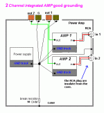
The PSU (middle diagram) is correct, particulary the note that voltage references go to the final ground symbol. That final ground is also shown correctly in the right most diagram between the three GND tracks.
The third layout diagram is wrong.
The input to each channel is a two wire feed.
The screen is that second wire and must connect to the input Signal Return pad on the PCB.
The extra wire from input RCA barrels to the PSU creates a LOOP in the two input circuits and will pick up interference. Remove that extra Loop.
The 10r "break resistor" as shown is dangerous.
You must not introduce a resistance into a potential Fault Current route.
That 10r cannot pass "Fault Current" to PE.
The Thread that contained that original diagram discusses this Safety in detail.
You can replace that resistor with a Disconnecting Network. Two inverse parallel Power Diodes can meet this duty. See esp for diagram.
The Speaker leads shown in green must be close coupled with the Speaker Return leads.
Add in the D.Joffe HBRR+HBRL for thos two channel amplifier.
Do NOT take any ground, or voltage, references to the smoothing capacitor junction !For best result, all ground should be connect between the two big capacitor of the power supply, look at the image.
The third layout diagram is wrong.
The input to each channel is a two wire feed.
The screen is that second wire and must connect to the input Signal Return pad on the PCB.
The extra wire from input RCA barrels to the PSU creates a LOOP in the two input circuits and will pick up interference. Remove that extra Loop.
The 10r "break resistor" as shown is dangerous.
You must not introduce a resistance into a potential Fault Current route.
That 10r cannot pass "Fault Current" to PE.
The Thread that contained that original diagram discusses this Safety in detail.
You can replace that resistor with a Disconnecting Network. Two inverse parallel Power Diodes can meet this duty. See esp for diagram.
The Speaker leads shown in green must be close coupled with the Speaker Return leads.
Add in the D.Joffe HBRR+HBRL for thos two channel amplifier.
Last edited:
You might consider to revisit another bootstrap amp. It is elektor Equin.
Yes, I have built that one. I think based on your post 🙂
Ah and what are your experiences with that? my idea re your amp is to test a quasi complimentary output. These seem to produce more second harmonics at the expense of higher odd harmonics. I don't know how that is so or could be so,Yes, I have built that one. I think based on your post 🙂
Ah and what are your experiences with that? my idea re your amp is to test a quasi complimentary output.
I don't like bipolar quasi-complementary. Tho I know many fancy the Quad 303 or the Naim clones.
- Status
- Not open for further replies.
- Home
- Amplifiers
- Solid State
- Here's a simple but very good sounding 50 watts amp.