The EF blows up if the amp is clipped. It took D.Self a few years to realise his mistake.Andrew, I don't agree with all your suggestions: -
- Q10's collector is grounded, therefore it is not modulated with signal and the Cob is a nonissue.
It's not about loss of maximum power. Base stopper work by increasing stability margins, for some operational conditions. 1r0 to 2r2 often good enough for output devices and 4r7 to 22r for driver devices. But go too far and that stability goes out the window.The main VAS transistor should be a low Cob video transistor type.
- Why do you say the driver base stoppers need to be reduced? How much voltage is dropped at full power?
Take an example.- If the purpose of putting a resistor into Q10's collector leg is for current limiting how big does this resistor need to be to stop it burning up? At a value it is going to be useful don't you think it will adversely affect slew rate?
assume Rc = 1k and Vdc = 37V
For worst case dissipation the effective impedance of the EF is set to match the 1k collector load.
The 37Vdc is dissipated over 1k+1k
and Pmax = 684.5mW
half in the resistor load and half in the transistor CE.
The transistor and the resistor survive since both see a MAXIMUM dissipation of <342.25mW
I have seen one Designer going to 10k and claiming that performance of his amp was not compromised. But many here disagree. There seems to be a consensus that most double EF requires as low a collector load as is necessary to survive abuse.
Last edited:
Hi Andrew
I don't see how your statement: "The EF blows up if the amp is clipped. It took D.Self a few years to realise his mistake."
Relates to mine: "Q10's collector is grounded, therefore it is not modulated with signal and the Cob is a nonissue."
I never bother using driver base stoppers with this topology and so long as the bias generator is bypassed properly and the PCB is laid out well I've never had any problems. 100R is probably the most popular value in this position and I've built other people's designs that use 100R without problems.
That's OK, you look at possible tweaks and decide from the evidence which direction to take.Hi Andrew
I don't see how your statement: "The EF blows up if the amp is clipped. It took D.Self a few years to realise his mistake."
Relates to mine: "Q10's collector is grounded, therefore it is not modulated with signal and the Cob is a nonissue."
I never bother using driver base stoppers with this topology and so long as the bias generator is bypassed properly and the PCB is laid out well I've never had any problems. 100R is probably the most popular value in this position and I've built other people's designs that use 100R without problems.
Mosquito, I just noticed that you don't employ the usual transistor that protects the VAS by sensing the voltage drop across the VAS emitter resistor. You really should add it, because with this topology if it clips and sticks to the rail it will burn up the main VAS transistor.
Andrew's resistor into the VAS helper transistor's collector will protect the helper but will do nothing to protect the VAS in the scenario above.
Andrew's resistor into the VAS helper transistor's collector will protect the helper but will do nothing to protect the VAS in the scenario above.
Sorry for delayed comment, I'm moving, and therefore my connection time is somewhat erratic..
I'm reading all comments, tips, and suggestions. Il will try everyone in LTSpice, and see what happens.
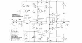
I suppose the third transistor in the VAS assy is the one that D.Self shows in the enhancesd Blameless in APAD 6th ed. ?
I do not unterstand why this Blameles, nor Elliot P3A show assymetrical clipping, competent designers vs lowly hobbyst (me) ? 🙂)
I'm reading all comments, tips, and suggestions. Il will try everyone in LTSpice, and see what happens.
I suppose the third transistor in the VAS assy is the one that D.Self shows in the enhancesd Blameless in APAD 6th ed. ?
I do not unterstand why this Blameles, nor Elliot P3A show assymetrical clipping, competent designers vs lowly hobbyst (me) ? 🙂)
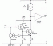
That's the one. R2 needs to be sized so that Q3 starts to conduct at the desired current limit for Q2.
This topology will always show very asymmetrical clipping due to the single ended voltage amplifier stage. If you don't like this then look at some other designs (Leach amplifier, etc.) with a push-pull VAS.
This topology will always show very asymmetrical clipping due to the single ended voltage amplifier stage. If you don't like this then look at some other designs (Leach amplifier, etc.) with a push-pull VAS.
Vr2 should remain below 400mV for all normal working currents.
Theoretically the VAS can vary by the bias current and a bit higher. eg, the VAS biased to 7mA can pass as little as 0.1mA and go very high to 20mA. I.e. the VAS current is 7mA -6.9 +13.
The current passing R2 could vary from 0.1mA to 20mA. You have to decide at what R2 current level you want the protection transistor (Q3) to start turning on.
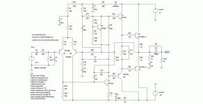
Nice simple amp. However, would like to see some sort of filtering and or regulation in the negative supply to the VAS. The reason is that there is coupling between the supply rail and the output of the VAS, thanks to the Miller capacitor used for stability.
The supply rails will likely be quite noisy, so this would probably offer a worthwhile improvement. OK, the input stage gain will reduce the effects thanks to the feedback, but it's something I personally would do.
The supply rails will likely be quite noisy, so this would probably offer a worthwhile improvement. OK, the input stage gain will reduce the effects thanks to the feedback, but it's something I personally would do.
Nice simple amp. However, would like to see some sort of filtering and or regulation in the negative supply to the VAS. The reason is that there is coupling between the supply rail and the output of the VAS, thanks to the Miller capacitor used for stability.
The supply rails will likely be quite noisy, so this would probably offer a worthwhile improvement. OK, the input stage gain will reduce the effects thanks to the feedback, but it's something I personally would do.
Yes, agreed, and I said as much in post #31. I find it odd that this RC filter often appears on the positive rail where the current sources are usually arranged (assuming conventional layout with PNP input transistors). I suggest 10R and 1000uF to maximize headroom whilst still keeping cap size sane.
Move the RC filter formed by R9 & C5 to the -ve rail, between the VAS and driver stage. The current sources arranged at the top will provide ample filtering (provided the Vrefs are stabilised) and filtering the -ve rail will improve PSR by reducing modulation of Cdom. D2 is probably best omitted.
EDIT: you probably won't see the benefits of this in simulation, because unless you tell it otherwise, the simulator "thinks" that the rails are fed from perfect voltage sources, which they aren't in real life, and will be subject to significant half wave rectification effects from the output transistors in particular.
Last edited:
EDIT: you probably won't see the benefits of this in simulation, because unless you tell it otherwise, the simulator "thinks" that the rails are fed from perfect voltage sources, which they aren't in real life, and will be subject to significant half wave rectification effects from the output transistors in particular.
I wast suspicious about that..
Ok, I followed most of the tips and advices suggested, resulting in great benefit on performance of the two circuits, the simplest one, and the enhanced one
Attachments
Yes, agreed, and I said as much in post #31. I find it odd that this RC filter often appears on the positive rail where the current sources are usually arranged (assuming conventional layout with PNP input transistors). I suggest 10R and 1000uF to maximize headroom whilst still keeping cap size sane.
OK, sorry, I missed that.
It seems to me that the effect of the very commonly used Miller C in the VAS is often overlooked. And of course, the positive rail isn't similarly afflicted - there's always a current source or bootstrapped load (as here), so no filter is needed.
As an aside, a few years ago I did a subjective comparison of a NAD 2130 (a 2030 without tone controls) and a humble Cambridge Audio A1 Mk3 (which uses integrated power amplifiers). The A1 sounded OK in isolation. Changing to the NAD was a revelation however. Using subjective terminology (!), I can only say that the difference was as follows: the A1 was characterised by the terms "veiled" and "wirey"; the NAD by "transparent" and "sweet".
These were not subtle differences - they were absolutely obvious. The thing that really got me is that I can remember these terms from the results of amplifier tests done in some of the HiFi mags of the 80s - yet here they were as the obvious descriptions of what I was hearing.
I wouldn't be at all surprised that the differences were due to the much superior power rails of the NAD.
(The tests were done using Quad ESL-57s).
Hi Mosquito, there is definitely scope there to improve performance with fewer parts.
You have a lot of large caps in certain positions. You should do some careful simulation because there might be some nasty surprises in store i.e. startup / shutdown transients and prolonged sticking on clip.
You have a lot of large caps in certain positions. You should do some careful simulation because there might be some nasty surprises in store i.e. startup / shutdown transients and prolonged sticking on clip.
Hi keith, I'm not familiar with these models but I wouldn't be surprised at all if better supplies led to better sound.
Another method I've seen used to reduce ripple injection from the supply rails via Cdom is to cascode the input pair and move the Cdom connection. But the RC filter is simple and effective, and avoids the possibility of instability that may arise from enclosing another transistor within the compensation network. If one were to cascode the LTP for other reasons (e.g. to use low noise, high beta, low voltage transistors in a high power amplifier) then the alternative Cdom connection would be worth a try.
Another method I've seen used to reduce ripple injection from the supply rails via Cdom is to cascode the input pair and move the Cdom connection. But the RC filter is simple and effective, and avoids the possibility of instability that may arise from enclosing another transistor within the compensation network. If one were to cascode the LTP for other reasons (e.g. to use low noise, high beta, low voltage transistors in a high power amplifier) then the alternative Cdom connection would be worth a try.
Maybe I was not aware of that because I carry square wave sims W/O input- output filters, and no rail caps, resistances, and diodes?You have a lot of large caps in certain positions. You should do some careful simulation because there might be some nasty surprises in store i.e. startup / shutdown transients and prolonged sticking on clip.
I thought I'd do a Spice simulation of a simplified version of the amplifier, with a noise source in the negative rail. Lo and behold, an ac analysis revealed that the response was only 27dB down at all audio frequencies. So, 4V p-p ripple (for example) on the negative rail will result in about 200mV p-p at the output.
I tried all sorts of variations, different transistors, cascodes, etc., but the only factor affecting noise response was the bootstrap capacitor - and removing it resulted in a dramatic improvement. Of course, this is due to the fact that the VAS gain will be drastically reduced without the bootstrap.
I think all amplifiers using this type of configuration would benefit greatly from proper decoupling in the negative rail. So my suggestion is that the R, C and diode in the positive rail should be duplicated in the negative rail.
Hi, I followed holmesc advice and put 10R 1000uF decoupling in the neg rail, between drivers and VAS. Now I'm working only in the simplest circuit, bootstraped, with no CCS, no current mirror. Only "refinement" is the three transistor VAS assy.
SQW response is good at (PULSE(-0.18 0.18 0 .01p .01p 25u 50u), I'm not sure how to check in a simulation how good/bad the amp left before a sporadic clipping on peaks..
SQW response is good at (PULSE(-0.18 0.18 0 .01p .01p 25u 50u), I'm not sure how to check in a simulation how good/bad the amp left before a sporadic clipping on peaks..
Fine with me if you want to tweak it to death 🙂 , but in the real world having, say, 1V assymmetry between positive and negative peaks is absolutely inaudible.
And the amp itself *is* not symmetrical anyway.
And the amp itself *is* not symmetrical anyway.
They told me why this type of circuit shows assymetrical clippinng, I understood, so this issue was left behind. I also understand that all this triple zeros performances will be ruined in the real thing by less than stellar pcb layout, cabling, and other practical issues. But this is a learning excercise in how's and why's...
- Status
- Not open for further replies.
- Home
- Amplifiers
- Solid State
- Here's a simple but very good sounding 50 watts amp.