jcx said:
I would route both power traces up the left side of the board (hugging the physical edge of the board with pwr and gnd tightly interleaved),
Thanks jcx,
I have tried before to move the PS traces/components and didn't like how the traces were getting longer and, in general, the way the board was looking. I would like to keep the basic layout as is, leaving the board size as close to 4" x 6" as possible (now it's 130mm x 95mm).
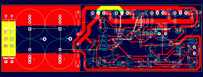
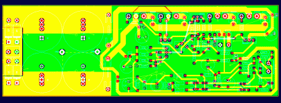
I have (finally) done some actual reading on ground layout and applied this (and the suggestions) to this latest layout. Once again, I have moved some components around. Notably, the speaker output and ground are further down the board.
Attachments
MJL21193 said:
Here are the latest:
OUTPUT--------------------AT 150 WATTS---------------AT 4 WATTS
20KHZ------------------------0.037--------------------------0.010
10KHZ------------------------0.007--------------------------0.002
5KHZ--------------------------0.002--------------------------0.001
1KHZ--------------------------0.001--------------------------0.000
50HZ--------------------------0.001--------------------------0.000
This is interesting: I changed the simulation models for the MJL3281A and MJL1302A for andy_c's improved models and the results are amazing. At 105 watts/20KHz distortion now shows 0.008% and 0.007% at 4 watts output.
That's a big drop for just changing the output stage models.
Hi,
is that large change in distortion performance an indicator of how reliable these simulation results are? Or to be taken with a pinch of salt?
is that large change in distortion performance an indicator of how reliable these simulation results are? Or to be taken with a pinch of salt?
Hi,
the advantage of ground over and around signals is one of signal integraty/EMC, it helps eliminate and decrease coupling between signals etc. A good source of information on grounding can be found looking for EMC/pcb layout related data, as the best defence against EMC is a board level (again I use EMC for both external sources as well as localised sources). Basicly as I've no doubt youve found out grounding can and is a PITA. There are numerous topographies for a circuit that will work, the problem is when a topology dos'nt work (and trying to find out why), and what we try to do is follow best practices to enshure we get oner that does work.
The mini planes I mentioned are for the positive/negative power inputs, fuse, capacitors.
The last couple of layouts look instintively more right from first impressions.
Must get internet back on at home as I seem to miss loads over the weekend and then have to catch up.
MJL21193 said:
At 105 watts/20KHz distortion now shows 0.008%
That's a typo - should read "150 watts/20Khz".
AndrewT said:
is that large change in distortion performance an indicator of how reliable these simulation results are? Or to be taken with a pinch of salt?
Hi Andrew,
To be honest, I didn't expect a change in performance from an update of the output stage models. That's why I didn't do it before - I thought it would be a waste of time. Apparently, I was wrong.
You have to ask yourself: "why would andy_c go to the trouble of creating new models for these?". The difference must be real, and if the sim says "better distortion", I believe it.
I had very serious doubts about the accuracy of the simulator at first, but now I'm learning just how good it is. After all, I worked up this amp design from several other designs and suggestions from other members, to a working prototype. Though not thoroughly tested, it behaves just as simulated.
Are the distortion figures accurate? Are they accurate for the SymAsym model I simmed? Or the Blameless? Or the KSA50? All of these show great distortion numbers. On the other end of the spectrum, I have modeled some amps that show dismal distortion performance (I will mention no names).
I think it's pretty clear that these simulation programs, and the results they present, should be accorded more respect.
MJL21193 said:Another take. Is there really any good reason for the gound plane over the small signal portion of the amp? I like this better (for what that's worth 🙂 ).
Yes there is a good reason, it helps at RF frequencies where our main concern is stability. Let's say you need to add a PS bypass cap somewhere in your circuit, the ground plane provides a low inductance path to ground anywhere it might be needed. It also provides a return path for RF fields.
You seem to be worried a lot about the gound near the large PSU caps, this involves 60 Hz and audio frequencies which are not critical much at all. You've removed the ground around the output devices which could oscillate at let's say around 1 to 100 MHz where a ground plane can be very helpful. Again, it is mainly for stability and high current capability.
Some here are applying RF theory, to audio and 60Hz signals where the effects are *much* smaller.
Again, it's your baby....
Pete B.
MJL21193 said:
That's a typo - should read "150 watts/20Khz".
Hi Andrew,
To be honest, I didn't expect a change in performance from an update of the output stage models. That's why I didn't do it before - I thought it would be a waste of time. Apparently, I was wrong.
You have to ask yourself: "why would andy_c go to the trouble of creating new models for these?". The difference must be real, and if the sim says "better distortion", I believe it.
I had very serious doubts about the accuracy of the simulator at first, but now I'm learning just how good it is. After all, I worked up this amp design from several other designs and suggestions from other members, to a working prototype. Though not thoroughly tested, it behaves just as simulated.
Are the distortion figures accurate? Are they accurate for the SymAsym model I simmed? Or the Blameless? Or the KSA50? All of these show great distortion numbers. On the other end of the spectrum, I have modeled some amps that show dismal distortion performance (I will mention no names).
I think it's pretty clear that these simulation programs, and the results they present, should be accorded more respect.
Many of the OnSemi models are completely broken in that they do not behave anything like the real parts. I believe that there are typo's or transcription errors in some of the models, they are way, way off. Many do not even bias up correctly or show beta droop anything like the real world. Sometimes one in a pair might be right with the other way off. Andy found more than one problem with the models:
http://www.diyaudio.com/forums/showthread.php?postid=1099978#post1099978
John - I'm not sure which you were using before.
Pete B.
PB2 said:
Yes there is a good reason, it helps at RF frequencies where our main concern is stability. Let's say you need to add a PS bypass cap somewhere in your circuit, the ground plane provides a low inductance path to ground anywhere it might be needed. It also provides a return path for RF fields.
Hi Pete,
I will go back to the drawing board and give it another try. I have been doing some reading on the subject, trying to educate myself.
One of the problems before was the large output trace that went from one side of the board to the other on the top layer. I've moved that to the bottom layer now, so it's not in the way. To avoid slots where I have made connections on the top layer, I will use jumpers here.
PB2 said:
Many of the OnSemi models are completely broken in that they do not behave anything like the real parts.
John - I'm not sure which you were using before.
In this post I showed the models from Multisim and On-Semi.
Looks like Bob offered a solution to the short circuit protection. You could use the opto isolator that connects to A and B to sense current and have it drive your relay directly. This provides direct current sense at the output devices:
http://www.diyaudio.com/forums/showthread.php?postid=1347801#post1347801
The set point is a function of Re, obviously, and what max current you want to allow for the outputs.
I've been thinking of floating a low supply voltage comparator between the Vbe supply and compare against a LV reference, which I think will provide a sharper limit curve and more variability in the set point.
Pete B.
PB2 said:Looks like Bob offered a solution to the short circuit protection.
Hi Pete,
Yes, I read him mention it in either that thread or another (PGP maybe). I was curious at the time about what he used.
I still like Rod's method better though, and in simulation, it can be calibrated to allow a certain amount of clipping. I'm thinking about a thermal switch mounted on the heatsink to protect the amp from overheating due to low impedance loads. Do you know a source for these? I'd need to determine the best shutoff temperature on the near completed amp, so no hurry.
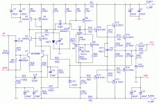
I have gone back to the drawing board, back to the schematic actually, to re-do the layout. I will be adding in the things I missed the first time around (such as terminal blocks). Also, Multisim has a neat feature that will calculate optimum trace width and pass this to Ultiboard. My first time using that feature so I don't know how well it works.
Here is the most recent updated schematic, showing all of the changes I made from testing of the prototype.
Attachments
MJL21193 said:
Hi Pete,
Yes, I read him mention it in either that thread or another (PGP maybe). I was curious at the time about what he used.
I still like Rod's method better though, and in simulation, it can be calibrated to allow a certain amount of clipping. I'm thinking about a thermal switch mounted on the heatsink to protect the amp from overheating due to low impedance loads. Do you know a source for these? I'd need to determine the best shutoff temperature on the near completed amp, so no hurry.
I have gone back to the drawing board, back to the schematic actually, to re-do the layout. I will be adding in the things I missed the first time around (such as terminal blocks). Also, Multisim has a neat feature that will calculate optimum trace width and pass this to Ultiboard. My first time using that feature so I don't know how well it works.
Here is the most recent updated schematic, showing all of the changes I made from testing of the prototype.
Hi John,
Yes, about the thermal sensor, I was about to say no it's not for low impedance loads, or a short for example. I say no because your amp does not have the SOA to handle low impedance loads, so heat sink temp is not fast enough. It's possible for a short to blow the bonding wires in less than a second which is not long enough for the heat sink to heat up. The fuses are far faster than a heat sink thermal sensor, as slow as they are.
The reason for a thermal sensor is that the output devices have to be derated as junction temperature increases. The amp can heat up for many reasons, driving low impedance loads, being in a poorly ventilated or even closed space, etc. The thermal sensor should trip when the heatsink temp goes beyond the temp that you used to derate the output devices, with some margin of course, see the picture here:
http://sound.westhost.com/project46.htm
http://www.cantherm.com/products/bimetal_cutouts/cantherm_bimetalcutouts.pdf
Pete B.
MJL21193 said:
Hi Pete,
Yes, I read him mention it in either that thread or another (PGP maybe). I was curious at the time about what he used.
I still like Rod's method better though, and in simulation, it can be calibrated to allow a certain amount of clipping.
The thing is that clipping is a voltage effect and what you want to protect, more importantly, is current. Really, you want both in terms of SOA, however if you have to choose one it would be current. The amp could clip all day into 8 or 16 ohms without a problem, yet the circuit would shut down. What about the amp at 75% power into 2 ohms? Would there be enough distortion to trip his circuit? Hard to predict.
The distortion circuit is good to light a clip light, as it was intended, but there are much simpler circuits for this.
Pete B.
PB2 said:
Hi John,
Yes, about the thermal sensor, I was about to say no it's not for low impedance loads, or a short for example. I say no because your amp does not have the SOA to handle low impedance loads, so heat sink temp is not fast enough. It's possible for a short to blow the bonding wires in less than a second which is not long enough for the heat sink to heat up.
PB2 said:
The amp could clip all day into 8 or 16 ohms without a problem, yet the circuit would shut down. What about the amp at 75% power into 2 ohms? Would there be enough distortion to trip his circuit? Hard to predict.
Hi Pete,
I wouldn't rely on the thermal sensor to detect short circuit - the clipping detection circuit would do that. Likewise, I wouldn't expect the clipping circuit to detect over load - the thermal switch would do that. Due to the limited SOA of the design, I'd want the temperature threshold of the switch fairly low.
In the simulation, the amp will reach ~170 watts into 8 ohms before clipping. This is ~250mV above the input sensitivity of the amp. The clipping circuit, during simulation, can allow another 200mV (or more) on input before it triggers. This leaves a lot of headroom before the clipping circuit opens the output relays. I see it as protection against hard clipping and short circuit, in case someone (me even 😉 )plugs some silly device in with an output greater than 2Vrms
PB2 said:
Thanks for the link. These are $1 from Digikey with temp ranges from 66 C to 240 C. Do you think 66 degrees C is too high for heatsink temp in this situation?
MJL21193 said:
Thanks for the link. These are $1 from Digikey with temp ranges from 66 C to 240 C. Do you think 66 degrees C is too high for heatsink temp in this situation?
Hi John,
60 to 70 C is usually what is used but it's hard to say without working out the details.
Pete B.
Originally posted by PB2
60 to 70 C is usually what is used
Thanks Pete,
I'll order a couple 66 degree ones anyway - just a couple of bucks.
I tried the rough prototype with Right Mark Audio Analyzer. It shows distortion from 20Hz to 20KHz to be 0.0156 at sound card input level voltage with a less than great attenuator on the output (a 250K pot). I am encouraged by this and I'll try this weekend to put together the better prototype, which follows the new layout.
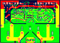
Layout. I'm working on it and it's going slowly (not big on doing the same thing over and over again). I have gone back to having the PS on the side. For the same size board (square cm wise), I get a more spacious component layout. I think I'll finally solve the ground plane problems with this one (as I have been told over and over but I'm a stubborn bull).
Live and learn, right?
Here it is in it's preliminary stage, with not copper laid down or the components in the best places.
Attachments
John,
I've mentioned that several of these grounding schemes should work well for an audio amp (LF), and that stability is the main consideration. I also mentioned that it has been noted by Cherry, Self and others that power and ground routing can impact distortion in the audio band when we are seeking ultra low distortion.
You seem to like Elliot's SIM circuit, why not use it to do a null distortion test with higher sensitivity and then see if the grounding and layout have any impact on measured distortion.
You are already quite low, so perhaps this is not an issue for you. I can understand that you might just want to build the thing.
Also, one more point I've been meaning to make. We both tried the VAS protection transistor, probably with a clamp point of perhaps 30 to 50 mA thinking that double the operating point is enough. Might want to try a set point of 100-200 mA something closer to the rating (SOA) of the device so that it is protected without increasing the distortion.
Pete B.
PB2 said:
I've mentioned that several of these grounding schemes should work well for an audio amp (LF), and that stability is the main consideration.
We both tried the VAS protection transistor, probably with a clamp point of perhaps 30 to 50 mA thinking that double the operating point is enough. Might want to try a set point of 100-200 mA something closer to the rating (SOA) of the device so that it is protected without increasing the distortion.
Hi Pete,
My motives for changing the layout were as much physical as electrical. I think these long narrow boards are a better fit in the chassis I have in mind. Also, I didn't like having the input stage smack dab in the middle of the board. With this current layout I don't have to worry about current flow, slots or any of the other troubles the other layout had.
If the Right Mark distortion analysis is reasonably accurate, I'm satisfied. My objective was not ultra low distortion , just as low as I could get it with a relatively simple circuit. I wanted it as good as the SymAsym, and from a simulation standpoint, it's exceeded that benchmark.
Have you tried the VAS protection at that higher current? I'll give it try later. Simplify things if the results are good (though it mucks up my layout 😡 ).
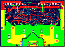
Here's the board with it's ground plane.
Attachments
- Status
- Not open for further replies.
- Home
- Amplifiers
- Solid State
- Help with this amp? A patchwork product of simulation