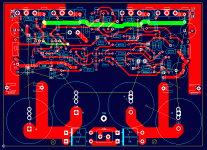
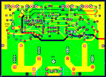
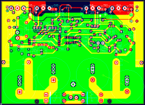
That was the top, full ground plane. Here is the bottom. I have gotten component placement about as good as I can manage. Of course, if I spent a few more hours going cross-eyed over it, I could probably improve it more. I'd like to say it's done now though, as I have already spent many glorious hours optimizing it.
Attachments
MJL21193 said:Here is the (slightly) modified circuit. I could use the NE5532's or a single quad. Rod advises that better performance results with a higher quality op-amp.
There is adjustment for sensitivity and will need to be calibrated. C20 could be changed to increase the amount of time the relay stays open.
Ah, interesting John!
I've been meaning to discuss this so it's good that you brought it up. You can see here that a typical fuse at 60% overload takes about 1.75 seconds to open, which puts us on the DC curve of the SOA chart:
http://www.intusoft.com/nlpdf/nl21.pdf
The relay that you've chosen, on the other hand, takes 15 mS to open, much better. I've been considering a circuit to monitor voltage and current and open such a relay if the output transistor SOA is exceeded which obviously includes simple current overload. One way to do this, for simple current overload only, is to characterize your power supply, lets say we know that at some target current say 5A the supply droops from 56 to 50 volts, we could divide the supply by 10 and compare to a 5V reference then open the relay with a timer to hold it open for say 10 sec to avoid relay chatter and to make it clear to the user that something is wrong.
Your circuit is quite good, and I understand that it should indeed work for say a short circuit, but you really want to allow the amp to go into say 5% clipping which is not very bad at all, and you certainly would not want to trip on one cycle of such overload. So if we set a reasonable threshold, then would it trip in time or at all when something like a 1 to 4 ohm load is used which would produce more distortion but perhaps not enough? The issue is that your trying to sense distortion as a measure of output current. Ideally, you'd sense supply or output current, supply droop as I suggested takes long with large supply caps so it is not ideal either. The output transistor emitter resistors are the obvious way to measure this without adding any losses, however you need a sense circuit that rides on the output signal.
Interesting problem, many possible solutions.
Pete B.
PB2 said:
You can see here that a typical fuse at 60% overload takes about 1.75 seconds to open, which puts us on the DC curve of the SOA chart:
http://www.intusoft.com/nlpdf/nl21.pdf
, but you really want to allow the amp to go into say 5% clipping which is not very bad at all, and you certainly would not want to trip on one cycle of such overload. So if we set a reasonable threshold, then would it trip in time or at all when something like a 1 to 4 ohm load is used which would produce more distortion but perhaps not enough? The issue is that your trying to sense distortion as a measure of output current.
Hi Pete,
Well, that is quite an in-depth analysis of fuse performance. That is a pretty elaborate model also. Multisim doesn't even use an actual model for fuses.
I thought that by going with a design that would provide roughly 3 times more power than I'd likely use, I'd avoid clipping.
I have some more simulations to run on the protection circuit, into reactive loads and low impedance loads to see what the sensitivity is. The last thing I want is for this to trigger during normal listening.
I want to use thermal protection to guard against overload from driving low impedance speakers. This would be fast, effective over-current protection, don't you think? I remember seeing a circuit somewhere using heatsink mounted diodes as the sensing device, originally to control a cooling fan. Adapt this to open the relay also.
I'll find it, I'm sure.
Hi,
firstly I must appologise if I seem to have posted earlier and then disapeared, I've been curled up on the couch glaring at some unbuilt speakers, and coughing for England. Been trying to keep up with all thats happened over the last few days (only have internet access at work at the moment.)
The layouts looking better. A way of picturing your ground is to print it iut and use coloured pens to draw where the currents will flow, use red for high current with big arrows and different colours and samller arrows for other area's, you'll soon see area's of conflict and also bottle necks, which usualy equate to inductors and need to be avoided.
Have you thought of SMD for the control (non-power) components, SOT23's and 0805 comps arn't to bad to place by hand, and the big advantage you get is reduction in area the circuitry takes giving you more room to be creative with the grounding. Often on two copper layer designs you have to compramise your design due to lack of space etc, adding 4 layers makes things much easier as you can have a bespoke ground layer.
marce said:
A way of picturing your ground is to print it iut and use coloured pens to draw where the currents will flow, use red for high current with big arrows and different colours and samller arrows for other area's, you'll soon see area's of conflict and also bottle necks, which usualy equate to inductors and need to be avoided.
Have you thought of SMD for the control (non-power) components,
Hi Marc,
I wondered what became of you.🙂
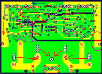
I have done what you suggested with a slightly modified layout. I see that current flow could be improved. I have used 3 colours for the arrows - red=high current, blue=medium current and pink=low current. I see that around the speaker output (circled in red) could be improved. Problem there is the component placement is tight and I wanted to tap into the output (big green trace) as close to the centre as possible. I could move this closer to the edge of the board, switching places with the VAS and driver that's there now. I'll work on this.
I could also bridge the copper in the other area circled, to allow the current from that area to flow down.
I would like to avoid SMD"s on this one. Let me become at least capable with through hole before I jump up to surface mount.😉
4 layers??? I'm having enough trouble with two!

Attachments
Hi ,
4 layers can and often is easier than 2 layers, it gives you two layers for signals and 2 layers for power distribution, because of EMC, component densitiy we use 4 layer as a minimum these days, though still get the odd request to do a 2 layer, which generaly fails new european EMC tests as a lot of microcontroller bases stuff has an ARM core, so you put on of these in the middle of a board with psu and all IO on same board, then try and get a clean ground on 2 layers
I'll print out the bits that I've missed and have a look tonight, like PB2 said this is a good eductaional thread for all of us that havn't done this sort of stuff for years / want to do it.
I use the arrow trick to help visulise current flow on complex grounding schemes it helps me to see the ground plane as it works, visulisation is half of PCB design.
Have a look at the pic below. Look familiar? Found it here:
http://www.diyaudio.com/forums/showthread.php?postid=1346445#post1346445
The Saint doesn't have a problem putting the rails that way. I wonder what his ground scheme looks like...
http://www.diyaudio.com/forums/showthread.php?postid=1346445#post1346445
The Saint doesn't have a problem putting the rails that way. I wonder what his ground scheme looks like...
Attachments
Hi John,
two quick comments, I think the central ground would be better connected to the 'star point' in the middle near the caps(with quite a wide connection 0.5" at least), this avoids this return current travelling round the board and adding to the RED current (with the arrows where two current streems cross, if it was rivers paint it would be purple where they mix, the only place we want purple is at the 'star point').
I'd make mini planes for the power around the diodes caps and fuses.
Have a good weekend, I'm off to try (!) finish my %*%$££$ cabinets. And try and catch up with this thread, cos I'm going to have to get of my deriere and deciede on what amps I require as all the kids now want in thier bedrooms (and the ones that have left home in thier house)
a. daddy to build them some speakers
b. daddy to build them some amps
As most of the lads are into Hip Hop etc so I dont think delicate Single driver with valve amp is gonna do somehow.

marce said:
I think the central ground would be better connected to the 'star point' in the middle near the caps(with quite a wide connection 0.5" at least), this avoids this return current travelling round the board
I'd make mini planes for the power around the diodes caps and fuses.
Have a good weekend, I'm off to try (!) finish my %*%$££$ cabinets.
Hi Marc,
I will bridge the copper at that location as you suggest.
These mini planes, are they isolated from the rest of the ground plane? If so, why the fuses also? The diodes I can understand - switching noise.
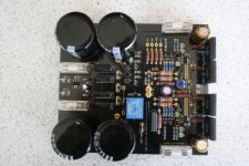
I'm feeling very good about the layout now, and after I implement the changes you've recommended, I believe it'll be ready for a prototype. For this, I may (for the first time) make my own board using Tom Gootee's method.
I'm PUMPED!
🙂 😎
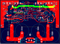
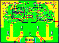
Ground plane layout again. This may look tedious, doing this over and over but it's much better than being disappointed with the end result. When it comes to board layout, there's no such thing as over optimization.
I have learned quite a bit over the course of this thread so far. For that, it's worth the effort.
I have learned quite a bit over the course of this thread so far. For that, it's worth the effort.
Attachments
Something I haven't done for a while - distortion figures. This is based on the latest updated schematic (I'll post that soon) with changesI've made based on the results from the rough prototype.
Back in this post, I listed the distortion figures for several frequencies at 4 watts and 150 watts.
Here are the latest:
OUTPUT--------------------AT 150 WATTS---------------AT 4 WATTS
20KHZ------------------------0.037--------------------------0.010
10KHZ------------------------0.007--------------------------0.002
5KHZ--------------------------0.002--------------------------0.001
1KHZ--------------------------0.001--------------------------0.000
50HZ--------------------------0.001--------------------------0.000
A reasonable increase in performance. Distortion is truely low. As I have said before, I have not modeled any amp that has reached these numbers.
I had planned to model the PGP, which is a low distortion amp, as a reference. It is very complex though, and would take a considerable amount of time.
I'm sure you really don't want to hear my ideas on proper power/gnd distribution at this late date but all of the layouts have a fundamental flaw - with a AB otuput stage you really don't want the highly distorted mag fields from each conducting phase' power supply current source and return paths to sweep over your small signal amplification feedback circuits as the output stage commutates
a way to mitigate this is to distribute the power gnd and power traces in a highly interlaced bus from one side of the board, global symmetry is not your friend in this instance - local symmety such as star quad or balanced microstrip are since they increase the order of mag field redution with distance
and the last layout violates the divided/slotted gnd "prime directive" - do not have power trace cross gnd plane gaps
jcx said:I'm sure you really don't want to hear my ideas on proper power/gnd distribution at this late date
Hi jcx,
Better late than never.🙂
One of my biggest disappointments here has been an almost total lack of interest from those "in the know".
I can make more changes, that's no problem. If the changes are needed to improve the layout, I won't hesitate.
Could you be a little more specific - are you referring to the big output trace?
Is there any way you could illustrate what you mean using my latest layout?
unfortunantly many confilicting goals require trading off in layout - a 1st question is the overall system gnd/power scheme - is each board power supplied from a separate transformer/set of windings? different choices result from considering a single channel in isolation and the problem of a common power source for multiple channels with nonisolated single ended source; balanced source/recivers for each channel restores more flexibiltiy, equivalent to separate power supplies/ch - illustrating the complexity of the trade-offs
I think Bill Whitlocks's seminar note is the best source for system level insight, I'd have to look for good board layout refs, but the system issues that Whitlock explains are still useful princples - follow the current - and its return path(s), "guesstimate" the mag field coupling and iterate
http://www.jensen-transformers.com/apps_wp.html
jcx said:
a 1st question is the overall system gnd/power scheme - is each board power supplied from a separate transformer/set of windings?
I think Bill Whitlocks's seminar note is the best source for system level insight, I'd have to look for good board layout refs,
Thanks jcx,
As for the power transformer: what I have right now is a single 40-0-40, 750VA that will power two channels. What the future has in store, that's a different story. I'd like an amp board that will give great performance despite other power factors.
I have looked over the material on the link you posted. A lot of good information.
I also did a little searching for ground plane implementations, especially with your comment about slots crossing power traces. I found this:
http://www.hottconsultants.com/techtips/tips-slots.html
With that in mind, I came up with this:
Attachments
It looks like you are planning on a balanced receiver type differential input (requires low impedance drive from a active filter or buffer after the volume pot)
This helps with a single ps xfmr – “dirty” power return gnd will be common at the xfmer CT/dual sec junction, the return currents in the pwr gnd wiring will give a V diff between pwr gnds on the two boards
The pwr gnd resistance should be minimized – bigger wire, multiple pwr gnd wires, wide pwr gnd trace on the pcb all reduce the V diff with current flows
The differential input amp front end can give ~40 dB (better with R matching) cancellation of this pwr gnd noise – the feedback, speaker gnd are at the end of “dirty” gnd path, the diff input translates/refers the input signal to the local dirty gnd at each board
So I would think of the power distribution to each board as a line with xfmr to the left: xfmr/wiring – pcb rect/filter C – output devices - speaker return constitutes the “dirty gnd/power path
The speaker terminals (speaker out and its gnd return should be as close together as practical) constitute the dividing point in this scheme: to the right of the speaker output terminals you then have a local low level signal amplifier circuit gnd where the feedback divider is connected to the speaker terminals and the differential input enters – all of the currents in this region should be nice linear versions of the audio signal since all of the drive/amplifier circuitry should be operating Class A
You probably want to bend this line into a horseshoe shape on the board
I would route both power traces up the left side of the board (hugging the physical edge of the board with pwr and gnd tightly interleaved), divide the gnd plane with a slot from the bottom edge to the speaker output and gnd terminals (these should be as close together as practical) at the top right edge of the board
Gnd plane slots are useful, especially at audio frequencies where trace/gnd resistance is the prime determinant of current flow and careful design of the gnd returns for high current/dirty supplies requires restricting the low resistance gnd return path to lie directly over/under the power traces – in fact it is probably better to think of the high power distribution+gnd trace as a low radiation cable implemented on pcb up to the output devices/speaker terminals – only on the low level circuit side does it really become a plane
- Status
- Not open for further replies.
- Home
- Amplifiers
- Solid State
- Help with this amp? A patchwork product of simulation