MikeB said:
The mjl3281 model from onsemi is useless bad. Try the mjw0281/0302 models, they work very fine.
Mike
Hi Mike,
I don't think it's a problem with the MJL models (they are in the multisim library).
The model is different than the one available from On-Semi.
This is the On-Semi model (from the web page):
**************************************
* Model Generated by MODPEX *
*Copyright(c) Symmetry Design Systems*
* All Rights Reserved *
* UNPUBLISHED LICENSED SOFTWARE *
* Contains Proprietary Information *
* Which is The Property of *
* SYMMETRY OR ITS LICENSORS *
*Commercial Use or Resale Restricted *
* by Symmetry License Agreement *
**************************************
* Model generated on May 3, 07
* MODEL FORMAT: SPICE2
.MODEL Qmjl3281a npn
+IS=8.26882e-10 BF=97.5769 NF=1.27505 VAF=63.6913
+IKF=7.75466 ISE=7.44075e-12 NE=3.39947 BR=0.1
+NR=1.6501 VAR=7.8831 IKR=15.9415 ISC=4.16531e-13
+NC=3.98207 RB=1.0642 IRB=2.65716 RBM=1.0642
+RE=0.0001 RC=0.051212 XTB=0.82132 XTI=1
+EG=1.206 CJE=1.10527e-08 VJE=0.677092 MJE=0.394732
+TF=1.93853e-09 XTF=1000 VTF=4.32084 ITF=149.92
+CJC=1.00256e-09 VJC=0.924803 MJC=0.524843 XCJC=0.100008
+FC=0.8 CJS=0 VJS=0.75 MJS=0.5
+TR=1e-07 PTF=0 KF=0 AF=1
Here is the one from Multisim:
**************************************
* Model Generated by MODPEX *
*Copyright(c) Symmetry Design Systems*
* All Rights Reserved *
* UNPUBLISHED LICENSED SOFTWARE *
* Contains Proprietary Information *
* Which is The Property of *
* SYMMETRY OR ITS LICENSORS *
*Commercial Use or Resale Restricted *
* by Symmetry License Agreement *
**************************************
* Model generated on Jan 7, 98
* MODEL FORMAT: PSpice
.MODEL MJL3281A npn
+IS=6.5498e-11 BF=139.247 NF=1.00176 VAF=46.776
+IKF=10 ISE=7.75232e-12 NE=3.34341 BR=4.98985
+NR=1.09511 VAR=4.32026 IKR=4.37516 ISC=3.25e-13
+NC=3.96875 RB=11.988 IRB=0.111742 RBM=0.102914
+RE=0.00127227 RC=0.209833 XTB=0.115253 XTI=1.03146
+EG=1.11986 CJE=1e-07 VJE=0.4 MJE=0.450375
+TF=7.04629e-10 XTF=1000 VTF=2.06045 ITF=41.8156
+CJC=5e-10 VJC=0.4 MJC=0.85 XCJC=0.959922
+FC=0.1 CJS=0 VJS=0.75 MJS=0.5
+TR=1e-07 PTF=0 KF=0 AF=1
Besides this, the same model is giving stable results in the patchwork amp.
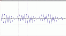
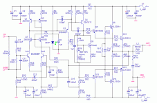
After some investigation, I've found the root of the problem originates with Q5 (from the schematic I posted above). The following graphic is what I see at it's base. This oscillation was reduced with a 220pF cap from Q5 base to collector.
What could be causing this instability?
Attachments
AndrewT said:Hi Mj,
are q7 base and r13/14 connected to the correct ground?
Which ground should the relatively clean c13/14/16/17 be connected to?
Where should r3 connect to?
Hi Andrew,
These grounding issues don't make much difference in the simulation. I know in the real world, they can make or break a design.
I have been working with this sim of the SymAsym for quite a while, but I didn't see this before because I didn't look in that particular place before. It doesn't show (much) in the output, and distortion figures are appropriately low.
marce said:
The ground scheme illustrated is the one on the left, it effectively a star ground but with low inductance planes rather than tracks.
(When you start throwing surface mount components on a board it is very very hard to do traditional star grounding dure to component sizes etc). the three legs of the ground plane correspond from left to right as follows.
Hi Marc,
I'm getting an idea of how you say the grounding should be. I have been studying my layout, trying to make it work.
One possibility is to do as 4fun suggests - move the supply caps and bridge back to the side of the board, rather than the bottom.
When I have a little more time, I'll try this. I will also increase trace width for the rails. Good tip with the caps across the rectifiers. Easy enough to tack those on the bottom of the board, if I'm too lazy to add them to the layout.
Hi John,
I think putting the caps and diodes on the other side is a good idea, that way you can have the caps and diodes linked by thier own local plane, this connected to the main plane on the top board by some decent through hole pin, or the return wire from the speakers. This would give you a definite star point and keep the diode capacitor noise localised. On switched mode PSU's it is critical that this loop is kept to an absolute minimum, due to the noise in it from the diode and the transformer winding switching, the same happens on 'linear' PSU's only at a much lower frequency, but at a more audiable figure.
Q5 base looks like AM, possibly a tranny base emmitter behaving as a diode somewhere in the circuit and feeding crud in. This is just an guess on my part though, but may help.
Just spent last 4 hours discussing the advantages of electro formed solder paste stencils (got a free lunch) so my brain is a bit numb!
marce said:Hi John,
I think putting the caps and diodes on the other side is a good idea,
Q5 base looks like AM, possibly a tranny base emmitter behaving as a diode somewhere in the circuit and feeding crud in.
I'll work on the layout tonight. Shouldn't be too difficult to move those. This may work out better anyway, as I would prefer a more narrow board. My great concern is with power supply traces behind the output transistors. Putting one supply on each layer might be the answer.
It's funny, with that sim of the Symasym, when I change Q5 to a higher current device, the oscillation goes away. I'm trying to understand why this could be, as this device is not conducting much current.
MJL21193 said:
I'll work on the layout tonight. Shouldn't be too difficult to move those. This may work out better anyway, as I would prefer a more narrow board. My great concern is with power supply traces behind the output transistors. Putting one supply on each layer might be the answer.
It's funny, with that sim of the Symasym, when I change Q5 to a higher current device, the oscillation goes away. I'm trying to understand why this could be, as this device is not conducting much current.
Symasym needs a Miller cap there IMO, the cap on the other device is not really a Miller cap. The larger device has more internal capacitance. Taking a look at the gain and phase margin might help with some understanding.
Pete B.
Hi John,
It has the benefit of very low inductance.
Also, regarding smoothing/decoupling caps:
Let all current pass the cap and not allow current to take a shortcut around it, i.e. all current should go through the pcb pad where the cap is soldered.
MJL21193 said:
Putting one supply on each layer might be the answer.
It has the benefit of very low inductance.
Also, regarding smoothing/decoupling caps:
Let all current pass the cap and not allow current to take a shortcut around it, i.e. all current should go through the pcb pad where the cap is soldered.
Here's a rough idea of how I'd do the layout, assuming these are your preferred X,Y dimensions:
http://baselaudiolabs.googlepages.com/board2.gif
Pete B.
http://baselaudiolabs.googlepages.com/board2.gif
Pete B.
MJL21193 said:
This oscillation was reduced with a 220pF cap from Q5 base to collector.
What could be causing this instability?
PB2 said:
Symasym needs a Miller cap there IMO, the cap on the other device is not really a Miller cap. The larger device has more internal capacitance. Taking a look at the gain and phase margin might help with some understanding.
Hi Pete,
I was beginning to think there was something wrong with the simulation program, which would seriously compromise the work and results accomplished in this thread.
Considering what happened when I put the cap from the base to the collector, and the outcome when I change Q5 to a higher current device, I have to agree with you.
Is it possible for the simulator to exaggerate this condition? That it may exist, but to a lesser degree?
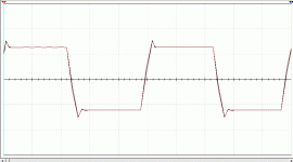
Here is a look at the same test on my simulation of the KSA50. Red trace is the signal input, black trace is the inverting input (feedback). No sign of instability.
Attachments
MJL21193 said:I have spent the afternoon testing the simulated amp (I dub it "Patchwork") and comparing it to the simulation of the SymAsym.
First I thing I did was to compare the signals on the inputs of the differential pair, to see if they match. For patchwork the sine wave comparison showed no difference, so I switched to squarewave. It shows a big overshoot on the leading edge of the inverting input (from feedback). To see if this was way off the chart as far as performance goes, I tested the symasym.
The results are below. Each is running a 20KHz squarewave at about 1/3 power output. There are two traces on each screen, each a different colour for A and B channels on the virtual oscilloscope.
My question is what is causing this overshoot? Is it normal or is there a way to reduce it? Will reducing it make a audible difference or is this just a stability concern?
Ideas? Comments?
Something doesn't look right there. Do you have an input filter on your design? I think SPICE is doing some odd things there, or it could be your design. I get a nice clean square wave with my power amp design, it looks perfect, and rings a bit with 1uF load on the output.
Pete B.
PB2 said:
Do you have an input filter on your design? ... I get a nice clean square wave with my power amp design, it looks perfect, and rings a bit with 1uF load on the output.
Pete B.
Hi Pete,
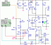
There is an input filter, and the O-scope is connected to the base of Q10 and Q11 (as shown below). There is an eight ohm load on the output (not reactive).
During that first test, I had left virtual probes in the circuit (these read current and voltage flow at a point in the circuit). As I mentioned before, these seem to cause problems with other readings. With these probes removed, I get a better result - not a perfect square wave, but one with a much cleaner and reduced overshoot. I will post the result next.
Attachments
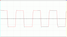
MJL21193 said:Here is the result. Input - 20KHz squarewave, 1.38Vpp. As pictured above, red trace goes to the base of Q10, green trace goes to the base of Q11.
That looks better, I didn't notice that you were looking at the differential input voltage, I was referring to the output voltage for my sims.
Pete B.
PB2 said:
That looks better, I didn't notice that you were looking at the differential input voltage,
I'm at a point in the design now where (with the simulation) I've exceeded my original goals. Performance, in my opinion, if as good as it needs to be. That's not to say "adequate", but I think we are at the point where further tinkering will will yield fewer and smaller gains.
The next step is to ensure the amp works as simmed.
As I have received the new transistors from Ampslab - the 2SA1011's. Although I still have not ordered the LM394's from Digikey, I started to prototype last night. I am halfway done, and should have it running (fingers crossed) by tomorrow.
Pictures soon. 🙂
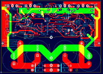
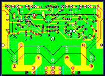
I spent some time working on the layout again. I tried it with the power supply components moved to the side, but found the results were not to my liking. First, increase in board size, due to the allowed size of the filtering caps. also, no improvement in rail trace length, there wound up being just as long.
I have been thinking about the ground scheme, especially the speaker return ground, and have come up with a few ideas.
First: on the board near the output transistors, there isn't any requirement for a high current ground. The closest component would be the .1uF bypass caps.
Second: Though the "hot" side of the speaker output is physically close to the output transistors, there doesn't seem to be any advantage in re-routing the ground to locate the speaker output ground close to it. In the end, this current has to travel to it's source anyway, whether it's via a trace on the board or through a wire.
Third: I like the idea of a separate high current ground on the board. I visualize the star point for the ground scheme off the board, on the chassis. With wires connecting the on-board high current ground, the on-board main ground and the speaker return ground, as well as the transformers cetre tap and the mains safety ground. Current , taking the path of least resistance, will exit the board and "dump" in the star ground.
Forth: Input signal is isolated on the board from the main ground by a 10 ohm resistor. The entire signal path from the board out will be isolated from any ground influence.
With these things in mind, I have been working with the layout last posted. I have made some changes - increased the output trace and the rail traces. I have retained the high current ground, but have kept it to a large trace rather than a plane. Not shown and yet to be added is the main ground plane. That I will post next.
Attachments
John,
Something to keep in mind is that while you want to minimize high current flow from the output ground to the input ground, you still want a low inductance connection, and only one if possible, between the two. The feedback loop encloses both the input and output sections, and if the grounds are not tight there is more potential for oscillation, or at least differences between sims and real life. The ground, obviously, is part of the feedback path.
One of the reasons for having a PC board and ground planes is to keep these paths short and low inductance, adding wires to a star point negates this advantage.
It is your baby, so I'll probably slow down now since I'm just repeating myself.
We were posting at the same time, don't quite follow your new ground plan there.
Let me offer something, if you wanted to model your ground plane, you could add an inductor (or transmission line) between every ground connection and simulation ground. The values of the inductors would depend on the length and width of the traces/wires. The goal is usually to minimize these inductances, especially for high frequency paths, keeping in mind interactions between the high current and small signal areas. I'm not saying to actually do this, but the thought process helps to select a better grounding scheme.
Pete B.
Tom Gootee did exactly this to allow users of his Spice simulation to investigate the effects of cables and traces on the quality of the four regulator scheme he posted.PB2 said:.............Let me offer something, if you wanted to model your ground plane, you could add an inductor (or transmission line) between every ground connection and simulation ground. The values of the inductors would depend on the length and width of the traces/wires. The goal is usually to minimize these inductances, especially for high frequency paths, keeping in mind interactions between the high current and small signal areas. I'm not saying to actually do this, but the thought process helps to select a better grounding scheme.
AndrewT said:Tom Gootee did exactly this to allow users of his Spice simulation to investigate the effects of cables and traces on the quality of the four regulator scheme he posted.
Been doing it for the last 10-20 years for high speed designs. In ASIC design we backannotate the physical characteristics resulting from the actual layout in support of detailed timing analysis.
Pete B.
PB2 said:
It is your baby, so I'll probably slow down now since I'm just repeating myself.
Hi Pete,
NO, don't go. It's not my baby, I'm just the guy with the nails and the glue.
The grounding is driving me nuts. At this point I think I'd almost be better off putting the power supply off the board.
I'll take another crack at that later
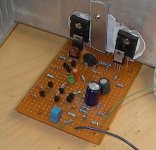
In the meantime, I've finished putting together the prototype. It's rough for sure but should give an idea whether this will work. I have tried it at 15 volt rails, and it produce some sound, though it's not quite right. All I get is treble, so I've done my usual trick and funked something up. I've checked some voltages and they match the sim fairly well.
I did it with only 1 output pair. This should be sufficient for testing.
Here's a pic. The outputs emitter resistors and the zobel are behind the "heatsink".
Attachments
MJL21193 said:
and it produce some sound, though it's not quite right. All I get is treble,
More testing.
The amp operates ok at the current limited 15 volt rails. I was mistaken about the output only being treble - somehow, at some time, I managed to burn out the woofer in my test speaker (a Koss 6x9 car speaker).
I tried it at +/-35 volts and I have a problem. It appears Q4 (VAS) is saturated. I have changed the value of R6 from 220R to 1K - this made no difference. I changed the two pole compensation to a single Miller cap - no difference. Changed the value of R4 - no difference.
I went back to the sim, tried different things to try to reproduce what the amp is doing.
I need some suggestions. There must be a simple answer to this that I just can't see (due to lack of complete understanding.)
Attachments
- Status
- Not open for further replies.
- Home
- Amplifiers
- Solid State
- Help with this amp? A patchwork product of simulation