Re: Re: Re: Re: Re: Re: Re: Re: VAS Protection
some quick key punches and we have ~1.6W dissipation in the VAS @ full power.
This goes up to ~5.8W when output is short circuited AND high level signal at the input.
the 2sa1011 can take about 16W @ 31Vce and about 8W @ 54Vce.
Think about the heat build up in the junction of the VAS.
1.6W dissipation with a small sink and you will find the Tc value and use that to de-rate the 54V dissipation for elevated temperature. You should find that this can be designed for.
Now put 5.8W through it and using that same heatsink find the new Tc if the short is prolonged. In this case the de-rated dissipation (SOAR) probably cannot be survived. You will probably need the rail fuses to blow to save the VAS. They will also protect the drivers from prolonged dissipation effects and may just save the outputs if a close rated F fuse is selected.
You may be able to use your input mute circuit with output current sensing to remove the drive to the VAS and Drivers to achieve similar protection from prolonged overcurrent, but the mute should have a delayed release to prevent chattering. It would be even better if repeated muting could be counted and then the mute latched to prevent overheating.
Note, that your use of a 25W VAS device saves the day, whereas a more normal 5W or 7W device will almost certainly fail for that simulated senario.
Hi,MJL21193 said:Under normal condition (152 watts into 8 ohm load) I get ~300mV across R41 and 54.4V through the VAS.
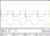
Here's how things look with the compensation changes you recommended and the output shorted.
some quick key punches and we have ~1.6W dissipation in the VAS @ full power.
This goes up to ~5.8W when output is short circuited AND high level signal at the input.
the 2sa1011 can take about 16W @ 31Vce and about 8W @ 54Vce.
Think about the heat build up in the junction of the VAS.
1.6W dissipation with a small sink and you will find the Tc value and use that to de-rate the 54V dissipation for elevated temperature. You should find that this can be designed for.
Now put 5.8W through it and using that same heatsink find the new Tc if the short is prolonged. In this case the de-rated dissipation (SOAR) probably cannot be survived. You will probably need the rail fuses to blow to save the VAS. They will also protect the drivers from prolonged dissipation effects and may just save the outputs if a close rated F fuse is selected.
You may be able to use your input mute circuit with output current sensing to remove the drive to the VAS and Drivers to achieve similar protection from prolonged overcurrent, but the mute should have a delayed release to prevent chattering. It would be even better if repeated muting could be counted and then the mute latched to prevent overheating.
Note, that your use of a 25W VAS device saves the day, whereas a more normal 5W or 7W device will almost certainly fail for that simulated senario.
Re: Re: Re: Re: Re: Re: Re: Re: Re: VAS Protection
Thanks Andrew for that evaluation. The VAS and drivers will be on a considerable heatsink, as I find they get quite hot during testing.
The short circuit protection will need to be looked at, but it must be accomplished off-board, as I have now done the FINAL revision of the circuit board layout.
Suggestions for the short circuit protection are always welcome.
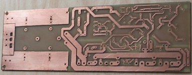
Lessons learned from the laser printer transfer say that the traces could be a bit wider and the clearances increased. I have applied these to this new layout, plus some of the other changes I did since the previous layout.
The FINAL version:
AndrewT said:~1.6W dissipation in the VAS @ full power.
This goes up to ~5.8W when output is short circuited AND high level signal at the input.
the 2sa1011 can take about 16W @ 31Vce and about 8W @ 54Vce.
You may be able to use your input mute circuit with output current sensing to remove the drive to the VAS and Drivers to achieve similar protection from prolonged overcurrent, but the mute should have a delayed release to prevent chattering. It would be even better if repeated muting could be counted and then the mute latched to prevent overheating.
Thanks Andrew for that evaluation. The VAS and drivers will be on a considerable heatsink, as I find they get quite hot during testing.
The short circuit protection will need to be looked at, but it must be accomplished off-board, as I have now done the FINAL revision of the circuit board layout.
Suggestions for the short circuit protection are always welcome.
Lessons learned from the laser printer transfer say that the traces could be a bit wider and the clearances increased. I have applied these to this new layout, plus some of the other changes I did since the previous layout.
The FINAL version:
Attachments

Re: Re: Re: Re: Re: Re: Re: Re: VAS Protection
Hi John,
We need a scope view of that, in order to see the peak values.
Pete B.
MJL21193 said:
Hi Pete,
I did as you asked and here are the results:
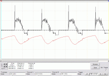
Under normal condition (152 watts into 8 ohm load) I get ~300mV across R41 and 54.4V through the VAS.
Here's how things look with the compensation changes you recommended and the output shorted.
Hi John,
We need a scope view of that, in order to see the peak values.
Pete B.
Re: Re: Re: Re: Re: Re: Re: Re: Re: VAS Protection
Here it is under normal conditions descibed above. Black trace (20mV/div) is voltage across R41, red trace (50V/div) is voltage across the VAS. Red trace is offset on the Y axis by -1.
PB2 said:
We need a scope view of that, in order to see the peak values.
Here it is under normal conditions descibed above. Black trace (20mV/div) is voltage across R41, red trace (50V/div) is voltage across the VAS. Red trace is offset on the Y axis by -1.
Attachments
I have etched my first board!
I must say this is very satisfying, doing things this way. Now, anytime I need a board for whatever reason, I can make one.
I used Tom Gootee's recipe of muriatic acid and peroxide. Wow, did it eat the copper quick! Only a few problems: the ground plane (top copper) didn't exactly line up with the bottom, and I spent a considerable amount of time last night scraping toner off around the through holes (I drilled these first).
Also, like I mentioned earlier, I didn't use enough heat to transfer the toner. The results are a rather rougher looking on the copper top with a few spots where the etchant started to eat through. I used a "sharpie" style marker (looks the exact same, Staples brand) but I guess it lacks that certain something that makes it resist acid. I also could have left it to etch for just a little while longer as there are some pin-pricks of copper still in a few places.
Next time I'll know better. I have also made a list of other problems and tips that I will address the next time round.
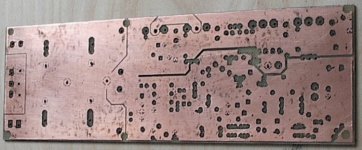
The bottom (looks good):
I must say this is very satisfying, doing things this way. Now, anytime I need a board for whatever reason, I can make one.
I used Tom Gootee's recipe of muriatic acid and peroxide. Wow, did it eat the copper quick! Only a few problems: the ground plane (top copper) didn't exactly line up with the bottom, and I spent a considerable amount of time last night scraping toner off around the through holes (I drilled these first).
Also, like I mentioned earlier, I didn't use enough heat to transfer the toner. The results are a rather rougher looking on the copper top with a few spots where the etchant started to eat through. I used a "sharpie" style marker (looks the exact same, Staples brand) but I guess it lacks that certain something that makes it resist acid. I also could have left it to etch for just a little while longer as there are some pin-pricks of copper still in a few places.
Next time I'll know better. I have also made a list of other problems and tips that I will address the next time round.
The bottom (looks good):
Attachments
MJL21193 said:The top (not so good):
Hi John,
for the first time round that is actually excellent work!
Nico
Nico Ras said:
for the first time round that is actually excellent work!
Thanks Nico, I'm blushing

I see it as practice. It will serve as the new prototype.
I used the same transfer method to put the silkscreen on and it almost looks like are real circuit board. I am going to start putting the components in and I'll be using the MJL21193/94 as the outputs on this one (I only have 4 each of the MJL3281A/1302A - save those for the final versions). I will also stick with the BD550's for the differential pair. I have the LM394's but I'd like to save those for the final versions.
I forgot to add fuse clips to the Digikey order, so I'll need to do some hunting through my scrap for ones.
I have been busy. 🙂
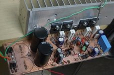
I populated the board, using MJL21193/94 as the outputs and a single LED as the cascode bias. Had some problems with fitting some of the components. I should have paid better attention to the sizes of everything, especially the terminal blocks.
I tried it out on +/-18 volts (bypassing the on-board supply). A steady +18 volts on the output - NOT good.
Spent a while trying to figure out why this was happening, looked for shorts and bridges. Finally, I went back to the schematic and board layout for clues. I found that, for some reason, the small signal transistors were back wards. 2N5550/5400 have EBC for 123, but the layout had it as CBE. Likewise for the BC550's - EBC instead of CBE.
That was slightly aggravating!
Turned these around and try again. Still stuck to the positive rail. Oops, forgot to turn around the EF before the VAS (2N5400). Try again - presto! Working!
I become encouraged by this success, and connect a 40-0-40 transformer, this time to the AC in on the board. Working very well, everything looks good.
With the VBE pot at around halfway, I see ~73mV across the emitter resistors on the outputs, which is about 270mA idle current.
Leave it going for a while, playing music at about 50 watts into a 4 ohm speaker. Heatsink (smallish) gets pretty warm and the drivers and VAS are almost too hot to touch. I'll need to construct some small sinks for these, ones that will fit in the cramped board layout.
Here's a shot of the bottom, with a look at my neat soldering. 🙂 Take note of my "special" fuses (black wires). Looked high and low, but I couldn't find any fuse clips. An excuse to make another Digikey order.😉
Attachments

MJL21193 said:
I added local feedback to the EF and VAS. This was something I was toying with earlier, but it got left by the wayside. This further reduced distortion by another .002%.
As quoted above, and referring to the latest schematic update, the feedback resistor was detailed as 100K. I found that to be too low, so I increased it, ending up with 500K. This value seems to work well.
Despite my big Digikey order, I'm still short some key components. Large among that are the fuse clips. I also don't have any quality 1uF caps. My supply of 1/4 watt resistors is getting low also, with the most common sizes almost gone.
I could only spare 2 6800uF power supply caps for this new prototype. That leaves me with 8 for the two final versions.
Here it is from the top. Pretty, ain't it?
Attachments
Anyone that has been following this thread could predict what I'm about to say... 😀
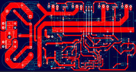
I have gone back to the drawing board and re-did the layout, again.
This time, I've taken a much more logical approach. I have made use of the lessons I've learned and put them to good use (hopefully) here.
I moved the drivers out to the main heatsink and shifted the speaker output terminal block close to the power supply caps.
I have oriented the emitter resistors on the outputs to lay flat. This provides more space to run the power traces.
I have re-sized many components to better fit on the board, such as caps, terminal blocks, resistors.
These changes didn't make much of a difference to the board size, but I think it's worth it. Besides, I hate a cramped board.
Attachments
Hi John,
congratulations so far, you must feel very proud
I only got up a few minutes ago so I am not yet sharp enough to make any meaningful comments but here goes.
On the new PCB did you change the lead-out of the small signal transistors like you discovered?
With the components behind the power transistors won't fitting to the heat sink be difficult?
I know making a symmetrical board looks nice, but I fear that when tempted to measure voltages you will short the positive supply to the ground via the heat sink with your probe. I would move this fuse a little more in-board.
I feel your input line is a little long, can you shorten it? It might be nice looking to have the input connected at the edge of the board but this may not always be good electrically.
Kindly show the board bottom as well.
Kindest regards
Nico
Nico Ras said:
congratulations so far,
On the new PCB did you change the lead-out of the small signal transistors like you discovered?
With the components behind the power transistors won't fitting to the heat sink be difficult?
I feel your input line is a little long, can you shorten it? It might be nice looking to have the input connected at the edge of the board but this may not always be good electrically.
Thanks Nico,
I did change the pins on this layout. I will double-check before I do anything else.
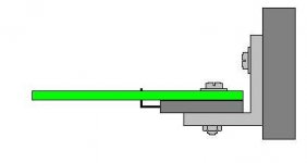
I have attached a sketch of how I'll attach this to the heatsink. I was also toying with a water cooling idea that I'd like to try out, but for now, it will be how it is in the sketch. Standard heatsink with either an aluminum or copper bar to give enough clearance.
This layout is still in it's first revision. I will implement more changes to this as I work with it. I am not happy with that front end arrangement either, and that will be my first change. I'll move that huge input cap to the outside, as before.
Any other recommendations would be appreciated.
Attachments

Nico Ras said:
Kindly show the board bottom as well.
Hi,
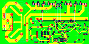
That is the bottom with the red traces. I will post the top here - a full ground plane with one slot. Also, bigger clearances around the through holes.
I have gone back and re-instated the feedback to the cascode. Further testing and listening shows no difference that I can detect with my ear or the meager equipment I have, so what's the harm? One resistor - it's there in case I want to take it out or leave it in.
This new prototype is so silent. No hiss while running or thump when it's turned on (just a slight cone movement). DC offset (with no signal, input not grounded) is less than 5mV.
The MJL21193/94's don't even break a sweat, driving my 3.1 ohm (Re) test speaker. A real work horse, these transistors.
Attachments
MJL21193 said:
Thanks Nico,
I did change the pins on this layout. I will double-check before I do anything else.
I have attached a sketch of how I'll attach this to the heatsink. I was also toying with a water cooling idea that I'd like to try out, but for now, it will be how it is in the sketch. Standard heatsink with either an aluminum or copper bar to give enough clearance.
This layout is still in it's first revision. I will implement more changes to this as I work with it. I am not happy with that front end arrangement either, and that will be my first change. I'll move that huge input cap to the outside, as before.
Any other recommendations would be appreciated.
Hi John,
I would like to make a suggestion since I don't know if hanging the PCB from your transistor legs is such a good idea. Place the transistors horizontally under the PCB (no need to change the layout). Then increase the board size so that you would sandwich the transistor between board and an L-bracket with its mounting screw. The L-bracket then mounts to the heat sink and it will bear the weight of the PCB completely. The L-bracket could be aluminium of about 2-3 mm thickness.
Attachments
MJL21193 said:
Hi,
That is the bottom with the red traces. I will post the top here - a full ground plane with one slot. Also, bigger clearances around the through holes.
I have gone back and re-instated the feedback to the cascode. Further testing and listening shows no difference that I can detect with my ear or the meager equipment I have, so what's the harm? One resistor - it's there in case I want to take it out or leave it in.
This new prototype is so silent. No hiss while running or thump when it's turned on (just a slight cone movement). DC offset (with no signal, input not grounded) is less than 5mV.
The MJL21193/94's don't even break a sweat, driving my 3.1 ohm (Re) test speaker. A real work horse, these transistors.
John,
the top ground link between capacitor legs is unnecessary, use the earth plane only and you can fatten the rail that squeezes between to be the same size as the other rail. Other than that I think it is a nice board.
Kind regards
Nico
One final word John, there is of course no rule that says that the tracks should be at the bottom of the PCB and earth at the top. If you swap your top and bottom layers around it would make a little easier assembly and there are only a few solder joints to the bottom. May solve some of the trough hole problems you had earlier.
Ciao
Nico
Ciao
Nico
Nico Ras said:
Place the transistors horizontally under the PCB (no need to change the layout).
Hi Nico,
The board would be supported at the heatsink either by standoffs from the case or mounting bracket on the heatsink. I like your idea though, and I think I'll use it, as it would simplify things.
Wouldn't the angle bracket reduce thermal transfer? Would a thicker angle be better?
Nico Ras said:
the top ground link between capacitor legs is unnecessary, use the earth plane only and you can fatten the rail that squeezes between to be the same size as the other rail.
The ground link is there to connect the bottom layer to the top, as I will be making these boards myself, I don't have through plating on the holes.
I will increase the size of the supply traces though, as big as can fit in this area.
Nico Ras said:One final word John, there is of course no rule that says that the tracks should be at the bottom of the PCB and earth at the top.
I'm stuck with this arrangement, as I won't have the through holes plated, near impossible to solder on the component side.
MJL21193 said:
Hi Nico,
The board would be supported at the heatsink either by standoffs from the case or mounting bracket on the heatsink. I like your idea though, and I think I'll use it, as it would simplify things.
Wouldn't the angle bracket reduce thermal transfer? Would a thicker angle be better?
John, my thoughts are that the thinner material would transfer the heat from the transistor to heat sink quicker as it does not introduce its own latency. But you need a very good thermal contact with both heat sink and transistor.
Again this is not a rule it is only experimentation that showed me this.
Kind regards
Nico
- Status
- Not open for further replies.
- Home
- Amplifiers
- Solid State
- Help with this amp? A patchwork product of simulation