Difficult to see where this distorion is generated, from this trace alone, but it seems to be of quite high order. (i.e. neither 2nd nor 3rd).
How is the open loop performance of your amp ? Diy you ever test it (careful when doing so because of DC offset and subsequent supply pumping) ?
Don't forget that the loop was designed for a filter whose cutoff frequency was almost an octave higher than the present one. You now have an unnecessarily low unity-gain frequency.
I'd suggest that you either use the output filter as determined or that we recalculate the components around the integrator.
The rectangular looks indeed cool, congrats ! How does the amp behave without load ?
Regards
Charles
Edit: What type(s) of OP-AMPs are you using and why did you go for 6 V pp for the triangular ?
Thanks (and sorry for the delay)!
Yes, you are right, I will correct the filter values so everything is as calculated.
About your question on the triangle amplitude, well, I chose a value not too low in order to more noise inmunity and not too high in order to have a smaller slew rate and less distortion in the circuit that generates it.
I use a low noise LM833 opamp for the error amplifier and a MAX038 for the triangle generator.
Best regards.
Hi,
Great thread guys. I'm looking forward to that paper on feedback too, there's some information to be found online about it of course but it's such a vast subject it's hard if not impossible to find a good spot for jumping in.
Cheers
Great thread guys. I'm looking forward to that paper on feedback too, there's some information to be found online about it of course but it's such a vast subject it's hard if not impossible to find a good spot for jumping in.
Cheers
It is basically ordinary control theory but I know that many people would be grateful to have at least some guideline.
Regards
Charles
Regards
Charles
I agree with you, this info can be very useful to any Class-D designer. I think Charles is the most helpful member in the forum. Congratulations. I hope that my experiments are helpful to somebody, too.
Pierre
Pierre
With 6 Volts pp @ 260 kHz you have 3.1 V/us slew-rate which might be a little large (with respect to the 7 V/us capability of the LM833) for comfort.
Regards
Charles
Regards
Charles
Truth
Charles is an extraordinary Element in CLASS_D Active Discussions. He simply accurate the phase of problem by applying its Indepth knowledge.
I regard and respect him as "Nelson Pass of Class-D"
He is extremely helpful as an active source of Information.
Without him I won't able to design some Class-D designs.
ThanX Charles for helping us.
regards
ampman
Pierre said:I agree with you, this info can be very useful to any Class-D designer. I think Charles is the most helpful member in the forum. Congratulations. I hope that my experiments are helpful to somebody, too.
Pierre
Charles is an extraordinary Element in CLASS_D Active Discussions. He simply accurate the phase of problem by applying its Indepth knowledge.
I regard and respect him as "Nelson Pass of Class-D"
He is extremely helpful as an active source of Information.
Without him I won't able to design some Class-D designs.
ThanX Charles for helping us.
regards
ampman
Do you think that the triangle amplitude/freq. is a bit high?
What would be the benefits of using a very high speed opamp as the error amplifier?
I think that, as the error signal is integrated and taken after the output filter, there is no need to have a very fast error opamp, at least with a very high slew-rate, right? (remember that, in my setup, the triangle goes directly to the comparator, it is not mixed with the signal and then the output is quantized like in other designs).
Thanks
PS: Charles, I can see that you are very appreciated in this forum. I didn't know because I am very new here, now I appreciate that I can feel lucky to count with you help.
It's probably better to take the feedback before the output fiter in a carrier type. In my simulations the phase shift of the output filter puts some nasty artifacts on the output waveform and also allows any switching risidule into the error amp so it spends it time correcting that aswell as the audio.
I got better results with a RC filter taken before the filter. I managed to obtain a 0.02% THD at 1kHz @ 1v in the simulation using this (I was using balanced modulators aswell... atleast I think thats what its called). This was done using the TL072 as my difference amp and error amp.
If you want to see the schematic just ask.
Good luck
Matt
In my simulations the phase shift of the output filter puts some nasty artifacts on the output waveform and also allows any switching risidule into the error amp so it spends it time correcting that aswell as the audio.
This artifacts are a general problem in carrier-based class-d amps. They can indeed be exagerated by after-filter feedback-takeoff. Thats why I asked Pierre if everything else was working nicely in the first place.
If you want to see the schematic just ask.
Yes please !
Did you also build it ? Keep in mind that you can have differences between simulations and real-life. In a simulation people usally use linear inductors, what they definitely aren't in real life.
I had better sonic results when playing around with post-filter feedback.
An alternative would be a mixed solution with pre- and post- filter NFB.
I used the TL 072 in a design 14 years ago (using a 250 kHz and 2V pp carrier) and it showed to be quite good for that purpose, although there would be better ones around nowadays.
Keep in mind that a class-d amp is a precision RF circuit used to process an audio signal.
Pierre wrote:
I think that, as the error signal is integrated and taken after the output filter, there is no need to have a very fast error opamp, at least with a very high slew-rate, right? (remember that, in my setup, the triangle goes directly to the comparator, it is not mixed with the signal and then the output is quantized like in other designs).
The fact that we differentiate the output signal (parallel C on the feedback resistor) and that the response of the NFB integrator turns flat above a certain frequency, will lead to a triangular signal at the output of the NFB op-amp as before, when it was a simple integrator fed by the output stage directly.
One does not necessarily need to differentiate the feedback signal up to infinity. One can play with a series resistor on the capacitor of the feedback branch that is between 1 and 10% of the NFB resistor's value. That's another option I would suggest to Pierre to try out.
And never forget that a class-d amp is somewhat an "EMC-hell" which can also lead to unexpected problems sometimes.
Regards
Charles
Well, I have added a 4.7k in series with the 56pF capacitor that was in parallel with the 68k fb resistor.
I have noticed no difference in the simulation, only a decrease of the phase margin from 65 degs to 59 degs. But I will have to test in real-life to see if distortion is reduced at least "by eye".
I re-checked the switching waveform of the amplifier and it looks simply perfect, with 50ns rise/fall time and no overshoot at all (all this measured with load connected and no signal).
Then should I really expect a smaller distortion with feedback after filter than with feedback before filter? Are there any other things to check?
Cheers.
Keep in mind the 0.02% THD was using a 10u cap accross the output and using ideal components. Having 10u accross the output attenuates signals above about 5k I think, lowering it to 1u gave it a wider response at the cost of THD. Right now it measures at 0.047% at 1v and 0.1% at full swing (1.9v input). swithcing frequency is about 190kHz.
I recently changed the error amp to an OPA627, I had it spare so it saves buying a TL071.
I havn't built it yet 🙁
National rejected my sample request for its half bridge driver so I'll have to get a different one from farnell *shudder*
I hope it helps
Matt
I recently changed the error amp to an OPA627, I had it spare so it saves buying a TL071.
I havn't built it yet 🙁
National rejected my sample request for its half bridge driver so I'll have to get a different one from farnell *shudder*
I hope it helps
Matt
Attachments
That seem quite good figures. I hope it can be the same or even better with feedback after filter, anyway. Are that results of simulations or real-life tests?
Cheers.
Cheers.
fr0st,
if you'll set some dead time in the simulation, THD will be worse, but closer to the reality.
if you'll set some dead time in the simulation, THD will be worse, but closer to the reality.
I have just realized that I have input coupling capacitors that are tantallum, hence with polarity, while the opamps are fed at +/-10V, so there is no DC bias at the amplifier input, only that I want to remove it from the source.
That's not very good, but can this capacitors -really- have a bad influcence on distortion (they even get reverse-biased in the - cycles of the input signal)?
Perhaps it would be nicer to use ceramic SMD non-polarized capacitors, right?
Thanks!
That's not very good, but can this capacitors -really- have a bad influcence on distortion (they even get reverse-biased in the - cycles of the input signal)?
Perhaps it would be nicer to use ceramic SMD non-polarized capacitors, right?
Thanks!
Salut Pierre
Yes, tantalum caps in the signal path can increase distortion, though not in the orders of magnitude that you can clearly see it on the CRO.
And don't use ceramics as audio frequency coupling caps, use polypropylene instead.
Regarding the missing D.C. path: It depends on the circuit and place, whether you have to use a path to ground. On an inverted input you usually don't (the NFB is already building a path to ground in this case) and on the non-inverting input you usually have to add a path to ground.
If you are unsure about that you can post the schematic.
Regards
Charles
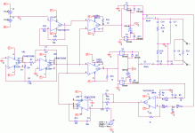
Of course I will post the schematics (although they are quite simple and I have revealed the details in this thread before), please let me time to draw them in the PC (I have it currently drawn by hand) and I will be very glad to post it here.
.
There is not a problem with DC, what I wanted to say is only that with the current design there is no DC in either pin of the input capacitors, so when the signal goes positive it gets reverse biased, nothing more.
What most puzzles me is the increase in distortion with respect to when I had feedback before filter (at least I couldn't clearly see it in the oscilloscope). The same input capacitors are there, and as I supposed and you have confirmed, they shouldn't have a visible influence. Perhaps the different L and C output filter values can have a lot to say there, but I sincerely doubt that's the only cause. And the PWM waveform looks great! Do you have an opinion on this, Charles?
Thanks!
.
Regarding the missing D.C. path: It depends on the circuit and place, whether you have to use a path to ground. On an inverted input you usually don't (the NFB is already building a path to ground in this case) and on the non-inverting input you usually have to add a path to ground.
There is not a problem with DC, what I wanted to say is only that with the current design there is no DC in either pin of the input capacitors, so when the signal goes positive it gets reverse biased, nothing more.
What most puzzles me is the increase in distortion with respect to when I had feedback before filter (at least I couldn't clearly see it in the oscilloscope). The same input capacitors are there, and as I supposed and you have confirmed, they shouldn't have a visible influence. Perhaps the different L and C output filter values can have a lot to say there, but I sincerely doubt that's the only cause. And the PWM waveform looks great! Do you have an opinion on this, Charles?
Thanks!
Salut Pierre
Is the problem persistent with the filter values the loop was originally designed for ?
Regards
Charles
Is the problem persistent with the filter values the loop was originally designed for ?
Regards
Charles
Wow! that's a fast response!
I haven't changed the values yet (I avoided it at a first start as they are heavily soldered and I didn't have the right soldering iron), but I will do for sure, hopefully this afternoon, and I will keep you updated!
Now it is 33uH + 1uF.
Thanks,
Pierre
I haven't changed the values yet (I avoided it at a first start as they are heavily soldered and I didn't have the right soldering iron), but I will do for sure, hopefully this afternoon, and I will keep you updated!
Now it is 33uH + 1uF.
Thanks,
Pierre
- Status
- Not open for further replies.
- Home
- Amplifiers
- Class D
- Help with feedback