40 mv sounds more reasonable.
The Vbe multiplier voltage sounds good up to now.
You have a single driver pair of driver transistors and then the output transistors pairs and so in order to turn all these on (and for bias current to flow) would need around 2.4 volts give or take. That is the vbe voltage needed in total for the four base/emitter junctions.
Have you tried adjusting the bias on the right channel? Does the preset allow you to go higher than the 2.325v you measured? The voltage you have is right at the point where the transistors should begin to conduct.
Hi,
Yes I've tried turning VR201 (bias adjusting trimmmer) in both ways, and the voltage goes lower and higher than the preset bias voltage at power on ; on the left board as on the right one.
I've checked the signal going at Q211 and Q212 bases in each amp : on the left board, I can see a nice sine wave, and a something like a square wave on the right amp.
But in order to check the earlier stage, where does this signal comes from ? I presume I will see it at Q206 and Q207 bases ? I'm not sure about which transistor does the class A amplifier's job, and where to look at this signal, sorry for that.
i'd be taking a hard look at c201 and c206 but that's me...
can you tells us exactly where in the circuit your probing to see your results?
can you tells us exactly where in the circuit your probing to see your results?
Hi,
Yes I've tried turning VR201 (bias adjusting trimmmer) in both ways, and the voltage goes lower and higher than the preset bias voltage at power on ; on the left board as on the right one.
I've checked the signal going at Q211 and Q212 bases in each amp : on the left board, I can see a nice sine wave, and a something like a square wave on the right amp.
But in order to check the earlier stage, where does this signal comes from ? I presume I will see it at Q206 and Q207 bases ? I'm not sure about which transistor does the class A amplifier's job, and where to look at this signal, sorry for that.
Concentrating on the bias issue for the moment, if you can raise the voltage across Q208 by altering the preset then you should be seeing the output transistors conduct and pass current. That increase in current will show as a voltage drop across the 0.47 ohm resistors.
The bias is a pure DC adjustment and as far as we are concerned does not depend on the stages before it. If you have sufficient voltage to bias those four B-E junctions into conduction then current should flow in the 0.47 ohms.
If this is not happening then you have a problem around the driver and output stage. There may or may not be other issues, but this lack of bias is something tangible that will respond to basic troubleshooting.
Hello,
C201 & C206 have been replaced, and boths are the same quality as in the left amp : Nichicon muse and Panasonic FC. I've have double checked them and they are good.
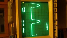
I've checked the output when turning VR201 to have more than 2.4V : there is no change, whatever I turn it down to 2.1V or up to 2.6V ; ie I have something "troncated" at the output, and weaker than the input signal, PP. There is a pic joined showing the output taken at the load. Sorry, I don't know why the pic has turned, its correctly orientated on my computer.
The signal take at Q206 & Q 207 collectors looks troncated too
C201 & C206 have been replaced, and boths are the same quality as in the left amp : Nichicon muse and Panasonic FC. I've have double checked them and they are good.
I've checked the output when turning VR201 to have more than 2.4V : there is no change, whatever I turn it down to 2.1V or up to 2.6V ; ie I have something "troncated" at the output, and weaker than the input signal, PP. There is a pic joined showing the output taken at the load. Sorry, I don't know why the pic has turned, its correctly orientated on my computer.
The signal take at Q206 & Q 207 collectors looks troncated too
Attachments
Last edited:
That looks like the upper driver/output isn't conducting, a problem that would give no bias and also still maintain a low DC offset like you have. It would also allow the vbe multiplier to generate a normal voltage.
All these things you have happening.
Before doing any thing else I would turn the bias preset to the end that give the lowest voltage across Q208. This will give minimum bias current which is the safest setting.
You need to check the continuity from Q208 collector to Q211 base which should read 220 ohms.
Check the connection from the emitter of Q211 to the base of the output transistors. Each should read 4.7 ohms.
Check the connection from the output transistor emitters to the central amplifier output line. Each output transistor should read 0.47 from emitter to this point.
If all that checks out OK then despite you showing around 500mv across B and E of Q211, its still possible this device is faulty.
Another possibility could still be a problem with the protection circuit. Removing D208 would isolate that section.
Ok, So all resistors and connections have been checked before taking voltages. Everything was OK.
500mV Vbe at Q211 is on the left amp (exactly : 585mV). Q211 Vbe = 4 mV on the right amp. And I've measured Vbe = 0.325V across Q212, on the right side. (Q212 Vbe = 0.585V on the left one).
I've also checked D208, desoldered, and it's good.
I think that at least a driver is toasted, and I have to change boths ?
Bad solder joints are a possibility, overheated driver transistors usually short. Check the voltage of the driver transistor collector lead versus the lead of the resistor driving the collector. If those are different there is a bad solder joint or fractured PCB trace (not unheard of). Or possibly the resistor pulling up the driver transistor opened up. I've had to bypass burnt out pcb traces with a wire sometimes.
Pamona grabber clips or the Q-ball originals are best for getting onto component leads without shorting leads together.
Pamona grabber clips or the Q-ball originals are best for getting onto component leads without shorting leads together.
Last edited:
I think You are talking about R222 / R223 ; same voltage on boths sides of these resistors, relative to ground. The only difference is between the two amps : +1.15V / -1.15V on the left one, +12.95V / -10.61V on the right one.
its also the voltages seen on the collectors of Q206 / 207.
its also the voltages seen on the collectors of Q206 / 207.
4mv across the B-E junction of Q211 suggests a problem. Its probably best to replace the pair although for fault finding you really just want to prove that is the problem.
Yes, everything leads to this ; I've checked also the pcb traces and nothing like a bad solder join. I have to desolder the drivers and check them.
unfortunately, I don't have these transistors in my stock, if they are bad, and couldn't find any good substitutes too.
I will order from the chinese / Singapore site "lcsc.com", discovered it when searching for the parts references. Very cheap !
They claim to sale real manufacturer's parts, and if it's true, they have KEC KTC4370A-Y / KTA1659A-Y.
You can see the real stock list, and choose between Singapore post or faster DHL shipping (they don't pay me to write this !)
For the price I will order the output transistors too, just in case...
As it will take some time to arrive, I will give report of the repair later.
Anyway, many thanks for the help !
Well, it's a bit strange : I've tested Q211 & Q212, Q206 & Q207, Q208, all desoldered, with a transistor tester, and also with a diode check on each pin (& reverse). All tests good, even in Hfe !
So the problem isn't coming from theses parts, isn't it ?
I'm not familiar with DC coupled stages in transistors amps (I'm a "tube guy" 95% of time), so sorry for these beginner's questions
Please would you confirm :
May I disconnect D208 & D209, as it seems to be part of the protection circuit, to see if it's the source of the trouble ? I mean without any risk for the amp (I've no DC on the output)
Am I correct to assume that Q207 is the VAS stage ?
Could the problem come from the differential pair ?
Removing D208 and D209 isolates the protection circuit. The risk is that if the amp draws excess current then there is no way for the circuit to limit that.
I would remove these (isolate one end of them) and just see if the fault changes. If it doesn't then resolder them back in place.
Q207 is the VAS.
The differential pair can cause many problems but it would be very unlikely to be at fault, and in any case would not cause lack of bias given the results you have posted so far.
Also can you try doing this... and the results do depend on the bias preset setting so be sure to adjust this to get a true reading. In other words turn the bias voltage up to a similar value to the good channel.
Connect your meter negative to the amplifier output and leave it connected here.
Now measure the DC voltage on the base of the upper NPN output transistor. It should be around plus 0.6 volts. Now check the voltage on the base of the upper driver NPN transistor. You should see around plus 1.2 volts.
Measure the voltage on the base of the lower PNP output and driver. These should be around negative 0.6 and negative 1.2 volts.
Grrr. I'm going nuts with this. And now on the defective board, I have no voltage at Q208 ! I mean Vbe and Vce = 0V.
During the measurement, I suddenly ear the relay click two times, as when the amp goes in the protection mode, and then reactivate. I've taken some voltages between output and ground : there is an erratic variation from 60 mv to more than 500mV.
everything is powered off, I will take a look at this on tuesday, double checking first the board, but for today I'm off !
Connect your meter negative to the amplifier output and leave it connected here.
Now measure the DC voltage on the base of the upper NPN output transistor. It should be around plus 0.6 volts. Now check the voltage on the base of the upper driver NPN transistor. You should see around plus 1.2 volts.
Measure the voltage on the base of the lower PNP output and driver. These should be around negative 0.6 and negative 1.2 volts.
Hello,
I'm back, after some soldering work... When I checked the transistors Q206 & Q207, I desoldered them, but I just forget to resolder one of them...
Resoldered since, and fortunately, without damage : The Vbe readings are correct, and I was able to adjust the Vbe multiplier output / bias voltage to the same level as in the good unit.
V base - output readings are, for the left amp (good unit):
Q211 "Upper" NPN Driver : +1.130V
Q221 "Upper" NPN Output : +0.535V
Q222 "Lower" PNP Output : -0.535V
Q212 "Lower" PNP Driver : -1.148V
V base - output readings are, for the right amp (defective unit):
Q211 "Upper" NPN Driver : +1.92V
Q221 "Upper" NPN Output : 0V
Q222 "Lower" PNP Output : 0V
Q212 "Lower" PNP Driver : -0.235V
open R222,R223? (220 ohm 1/4W)
and is R221 ok?
all these resistors (and the others too) are good
Your measurement would seem to indicate that you have 1.92 volts across the base/emitter junction of the upper NPN driver Q211. Yes 🙂
If so then Q211 is definitely faulty. There may be other issues but 1.92 volts across B-E shows that device is faulty.
If so then Q211 is definitely faulty. There may be other issues but 1.92 volts across B-E shows that device is faulty.
Well, the drivers are the "usual suspects", as the outputs.
unfortunately I have no good substitute in my stock, only some NPN/PNP output pairs : 2sc2525 / 2SA1075 and 2sc5200 / 2sa1943. A bit too much to drive the outputs ! But will it do the trick, just for a test ?
unfortunately I have no good substitute in my stock, only some NPN/PNP output pairs : 2sc2525 / 2SA1075 and 2sc5200 / 2sa1943. A bit too much to drive the outputs ! But will it do the trick, just for a test ?
- Home
- Live Sound
- PA Systems
- help with a defective InterM amp board