Ah that's right. I had to go grab one of my bare boards to verify. There's no trace between those two ground points on the PCB so you're correct. Need two wires back to power supply ground (if R22 and C6 are in use).There are 2 connections from the fe to GND.

I wonder if this behavior is the same on the other side of the circuit too.. D- and GND....Just tried to note the voltages at D+ and GND
Like I said it’s all over the place....
With the fe disconnected from the OS
D- and GND = -074.8
D+ and GND = -073.6
Not changing when I turn p2
D- and GND = -074.8
D+ and GND = -073.6
Not changing when I turn p2
Shall I reconnect the wires and try it on the D- side ?I wonder if this behavior is the same on the other side of the circuit too.. D- and GND....
Ya, I would get P2 back to a safe starting point before power up though. D+ and D- voltages should be stable, it's the biasing voltage that turns on the transistors in the OS.
No mate that was with everything connected.
As Papa is saying, in broader context - This is not Dialysis ........... but you really need to read and act as directed while troubleshooting, price for mistakes is quite high sometimes
Or you'll have some further ookup, and we all are deeper in tail chasing game
I did wrote "test just FE board"
My bad is that I didn't wrote "without OS connected"
So you didn't say anything smoked, so let's just hope nothing smoked when you dialed biasing on FE to max .........
now - without OS board connected to PSU and to FE, just test FE connected to PSU (both rails and GND)
again :
go back and test just FE board
test entire span of voltage between D+ and D- you can get fiddling with trimpot for biasing; red probe on D+, black probe on D-
also test span of voltages between D+ and GND, fiddling with DC Offset trimpot; red probe on D+, black probe on GND
write here what you got ......... and then we will know is it functional
after that we need to determine proper layout of OS connections - is everything in place (due to fingerpoking in past) and (hopefully) once again to confirm that all semis are functional
only then, with clear arrangement, is sane to go further\
so, please post pictures of your testing, so we can clearly see PSU wires; test both channels, write results specifically for each channel if there is difference
pics of both top and copper side of pcbs are welcome
one thing
if preaching choir is confusing, you can clearly say - "Boyz, hold on, I'm going to listen just that guy"
I would be happiest if some of Greedy Boyz who actually have same/similar amp at home, chime in and give some insight
even just picture of OS ensemble from same functional amp could be helpful, because I see those as potential problem, still
Ok , D- and GND = -066.3v this doesn’t change when I turn P2I wonder if this behavior is the same on the other side of the circuit too.. D- and GND....
D+ and GND = -064.8v p2 decreases the voltage when I reduce its resistance
This brings back memories of myself trying to teach my mother how to use windows 95 ! Now I’m the pupil 🤣As Papa is saying, in broader context - This is not Dialysis ........... but you really need to read and act as directed while troubleshooting, price for mistakes is quite high sometimes
Or you'll have some further ookup, and we all are deeper in tail chasing game
I did wrote "test just FE board"
My bad is that I didn't wrote "without OS connected"
So you didn't say anything smoked, so let's just hope nothing smoked when you dialed biasing on FE to max .........
now - without OS board connected to PSU and to FE, just test FE connected to PSU (both rails and GND)
again :
go back and test just FE board
test entire span of voltage between D+ and D- you can get fiddling with trimpot for biasing; red probe on D+, black probe on D-
also test span of voltages between D+ and GND, fiddling with DC Offset trimpot; red probe on D+, black probe on GND
write here what you got ......... and then we will know is it functional
after that we need to determine proper layout of OS connections - is everything in place (due to fingerpoking in past) and (hopefully) once again to confirm that all semis are functional
only then, with clear arrangement, is sane to go further\
so, please post pictures of your testing, so we can clearly see PSU wires; test both channels, write results specifically for each channel if there is difference
pics of both top and copper side of pcbs are welcome
Nothing connected to FE except D+ and D- and GND ( and out & GND speaker terminals)
D+ and D- = 000.2mv ( turning P2 pot does nothing)
D+ and GND = 2088mv and constantly dropping ( turning P2 pot does nothing)
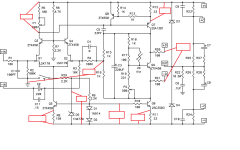
OK, if you're in the mood
Print this
inputs (both) shorted to GND, "T" closed (confirmed prior to powering on with ohmmeter)
connected PSU - both rails and GND, but no OS (leave it in other room)
measure DC Voltages for each red rectangle, write in rectangle
red probe is upper line from rectangle, black probe is lower line from rectangle
when all done and written in appropriate places, post here
Attachments
Thanks Zen , I’ll get on that tomorrow
Edit : that’s not me being lazy it’s because I no longer keep a printer, cyber cafe opens at 08:30 tomorrow.
Edit : that’s not me being lazy it’s because I no longer keep a printer, cyber cafe opens at 08:30 tomorrow.
Last edited:
you're faster with your one project, than I'm multitasking all of mine, and trying somehow to help here and there
so, no hurry, if I can say so ...... :clown
so, no hurry, if I can say so ...... :clown
Please confirm to this simple man if this is how I should be connecting the FE ?OK, if you're in the mood
Print this
inputs (both) shorted to GND, "T" closed (confirmed prior to powering on with ohmmeter)
connected PSU - both rails and GND, but no OS (leave it in other room)
measure DC Voltages for each red rectangle, write in rectangle
red probe is upper line from rectangle, black probe is lower line from rectangle
when all done and written in appropriate places, post here
Red ( positive from psu ) to V+ on FE
White ( neutral from psu ) to V- on FE
Inputs go to GND
I have tested the thermistor which before powering on is at 093.4 ohms which drops with heat ( hairdryer)
Last edited:
Well I so hope I have gotten this correct….OK, if you're in the mood
Print this
inputs (both) shorted to GND, "T" closed (confirmed prior to powering on with ohmmeter)
connected PSU - both rails and GND, but no OS (leave it in other room)
measure DC Voltages for each red rectangle, write in rectangle
red probe is upper line from rectangle, black probe is lower line from rectangle
when all done and written in appropriate places, post here
will have more time tonight
now - preliminary (first morning coffee then must fly) - it seems everything OK with FE
stare at goats OS-es, do not connect them to anything, we must deduce are there any errors with parts and what's proper termination of all lines to and from OS modules
something is very fishy about them
edit:
in meantime, you can do few more things with FE measurement:
- P1 - gimme measurements for both extreme positions (min and max) - repeat measurement across P1+R5 and write here (both cases)
- I assume P2 is in max position for this measurement; dial it all the way in other position, gimme measurement D+ to D-, write here
- write here Vdc for rails during the test; V+ and V-, black probe to GND in both cases
- same for C+ and C- points; I need to be sure these are appropriate before connecting OS modules
Last edited:
Revised readings :
I’ve tried really hard to understand where I’m to put the dmm red and black so I’ve attached another drawing showing where I had the red ( R ) and where I had the black ( B )
Staring at OS now Zen 👍🏻

I’ve tried really hard to understand where I’m to put the dmm red and black so I’ve attached another drawing showing where I had the red ( R ) and where I had the black ( B )
Staring at OS now Zen 👍🏻
In case this is important….
When I was sent the FE’s and their components the amazing other member substituted some transistors. ( all with the same pin outs )
2N5401 substituted by a ZTX550
2N5551 substituted by a ZTX450
KSC2690A substituted by a KSC3503
KSA1220A substituted by a KSA1381
When I was sent the FE’s and their components the amazing other member substituted some transistors. ( all with the same pin outs )
2N5401 substituted by a ZTX550
2N5551 substituted by a ZTX450
KSC2690A substituted by a KSC3503
KSA1220A substituted by a KSA1381
I can't help you with task of reading pcb against schematic
you alone must struggle and succeed in that, or you'll never be able to finish what you started
to repeat, and that's crucial for measurements - for each red rectangle I drew on schematic, there are two lines going from rectangle - upper one is red probe, lower one is black probe
when written "ref. to GND" that always means black probe to GND point ( anywhere in circuit, but most sure at pad where GND wire coming to pcb)
for now, I see fishy value across P1+R5
take your time, do it properly, or it will be no-go, you'll have door-stopper instead of singing amp
- Home
- Amplifiers
- Pass Labs
- Help please with my poorly Stasis 2